
Amplifier Circuit
Index 68
CURRENT_SUMMING_OPERAIIONAL_AMPLIFIER
Published:2009/7/14 21:12:00 Author:May
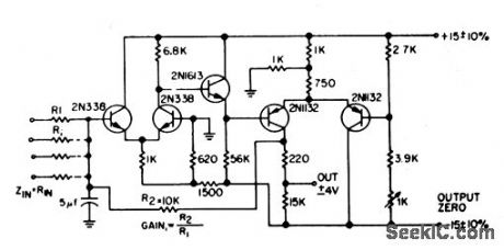
Uses current-summing to hold voltage at input node R1 at 0V. With more than one input, there is exact summation of inputs, with no interaction. As sine-wave amplifier, gain is 1,000, and bandwidth for transistors shown is d-c to 20kc.-C. J. Ulrick, Minimum. Interaction Summing Amplifier, EEE, 12:2, p 30. (View)
View full Circuit Diagram | Comments | Reading(1798)
12_V_AUDIO_AMPLIFIER
Published:2009/7/14 23:59:00 Author:Jessie
Input sensitivity is 10 to 20 mv for 0.5 w output. Maximum power output at 10% harmonic distortion is 500 mw. Design calculations are given.- Transistor Manual, Seventh Edition, General Electric Co., 1964, p 246. (View)
View full Circuit Diagram | Comments | Reading(971)
12_W_TRANSFORMERLESS_AMPLIFIER
Published:2009/7/14 23:56:00 Author:Jessie
Uses two transistors in parallel for each of theoutputs, to cut saturation resistance in half and thereby increase power output.Parallel operation also serves to reduce distortion. Operating efficiency is 67% at 12 w.- Transistor Manual, Seventh Edition, General Electric Co., 1964, p 267. (View)
View full Circuit Diagram | Comments | Reading(763)
TELEMETRY_SUMMING_AMPLIFIER
Published:2009/7/14 21:10:00 Author:May
Uses differential dual-triode first stage, voltage amp lifer, and current and voltage-limited cathode follower to give output swing of 5V above and below 0. Open loop gain of 2,000 is obtained with positive feedback in last two stages. Used to isolate transducers and to amplify d-c or low-frequency signals in air. borne or ground-based telemetry systems.-L. S. Klivans, D-C Amplifiers for Control Sys terns, Electronics, 31:47, p 96-100. (View)
View full Circuit Diagram | Comments | Reading(1008)
LOW_NOISE_AUDIO_AMPLIFIER
Published:2009/7/14 23:53:00 Author:Jessie
Power gain is 44 db, input impedance 440,000 ohms, and hum and noise 57 db down for 3-db frequency response of 20 to 100,000 cps.-L. E. Clark,E. B. Mack, and R. C. Heihall, High-lights of Small-Signal Circuit Design,Electronics, 36:49, p 46-50. (View)
View full Circuit Diagram | Comments | Reading(977)
STARVED_D_C_AMPLIFIER
Published:2009/7/14 21:09:00 Author:May
Serves as wideband input stage for chopper-stabilized amplifier that resolves 10 microvolts. Bandwidth is 100kc, equivalent input noise is less than 10 microvolts rms, and input current is only 8 nanoamperes. -Starved DC Amplifier Has Low Noise, High Z, Electronic Circuit Design Handbook, Mactier Pub. Corp., N.Y., 1965, p 108. (View)
View full Circuit Diagram | Comments | Reading(1326)
TEMPERATURE_COMPENSATION
Published:2009/7/14 21:07:00 Author:May
Sensistor silicon resistors in cross-coupling network compensate for tempensate changes. Circuit operates at resolution rate above 5 Mc if input pulse is above 10 v when pulse width is decreased from 100 millimicrosec.-How to Compensate for Temperature Variation in a Transistorized Flip-flop (Texas Instruments ad), Electronics, 33:37, p 97. (View)
View full Circuit Diagram | Comments | Reading(0)
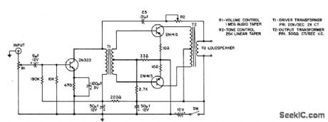
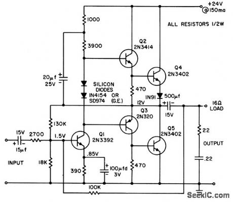
15_W_TRANSFORMERLESS_AMPLIFIER
Published:2009/7/14 23:47:00 Author:Jessie

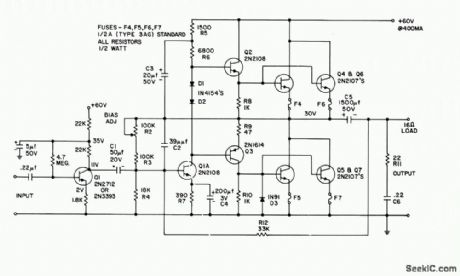
Uses additional input stage to increase input impedance from 3K to over 200K.Power frequency response is flat within 0.5 db from 20 cps to 20 kc. Output impedance is less than 0.3 ohms, for good speaker damping,and harmonic distortion at full power is less than 0.25%.- Transisfor Manual, Seventh Edition, General Electric Co., 1964, p 269. (View)
View full Circuit Diagram | Comments | Reading(1030)
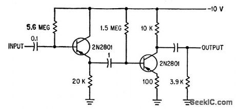
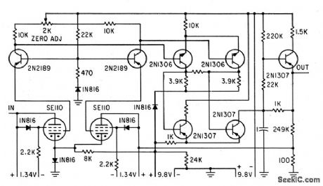
POWER_SUMMING_D_C_AMPLIFIER
Published:2009/7/14 21:05:00 Author:May
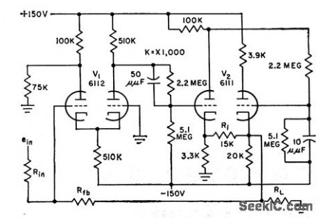
Open loop gain is 2,000 and maximum voltage swing is 10V into 2,000-ohm load. Maximum dosed-loop gain should be 50 for good stability. Used for straight resistance summing of several input signals.-L. S. Klivans, D.C Amplifiers for Control Systems, Electronics, 31:47, p 96-100. (View)
View full Circuit Diagram | Comments | Reading(814)
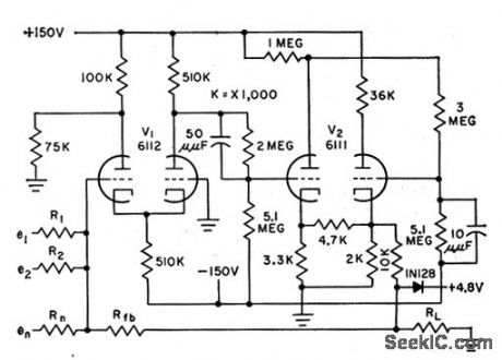
OPERATIONAL_D_C_AMPLIFIER
Published:2009/7/14 21:04:00 Author:May
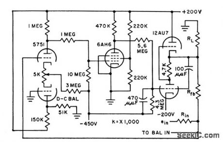
Ideal for control systems and analog computers because of broad passband and large control-system response characteristic. Open-loop gain above 15,000. Output swings 100V into 20,000-ohm load. Can be used from d-c to 20kc at unity dosed-loop gain.-L. S. Klivans, D-C Amplifiers for Control Systems, Electronics, 31:47, p 96-100. (View)
View full Circuit Diagram | Comments | Reading(851)
4OO_CPS_SUMMING_AND_POWER_AMPLIFIER
Published:2009/7/14 20:58:00 Author:May
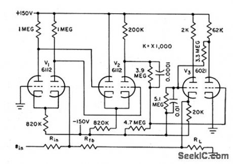
Used in either 60 or 400-cps control systems in which several signals must be summed and amplified in precise manner. Also used for broadband equalization when load impedance is below 25,000 ohms and phase lag must be minimum. Phase shift is less than 5° from d-c to 400 cps. Open-loop gain is above 5,000.-L. S. Klivans, D-C Amplifiers for Control Systems, Electronics, 31:47, p 96-100. (View)
View full Circuit Diagram | Comments | Reading(814)
BUILDING_BLOCK_AMPLIFIER
Published:2009/7/14 23:42:00 Author:Jessie
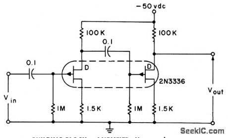
Has voltage gain of 1,000 and gain-bandwidth product of 15 Mc. High-fidelity audio preamp can be designed with two such packages, one with equalization network and one with tone control network.-L. J. Sevin, Jr., Field-Effect Transistors, McGraw-Hill, N.Y., 1965, p 74. (View)
View full Circuit Diagram | Comments | Reading(834)
STRAIN_GAGE_AMPLIFIER
Published:2009/7/14 20:56:00 Author:May
Battery-powered circuit for low-impedance transducers has voltage gain up to 10,000 with low noise and low drift.-D-C Amplifier uses Solion Tetrodes, Electronics, 35:39, p108. (View)
View full Circuit Diagram | Comments | Reading(0)
6_MSEC_TO_15_SEC
Published:2009/7/14 23:38:00 Author:Jessie

Provides continuously variable delay having good settability over entire range due to use of single log-tapered pot R1.-S. G. Freshour, Wide-Range Variable Delay Circuit, EEE, 14:3, p62. (View)
View full Circuit Diagram | Comments | Reading(775)
INPUT_CHANGE_RATE_TRIGGERED_RELAY
Published:2009/7/14 20:53:00 Author:May
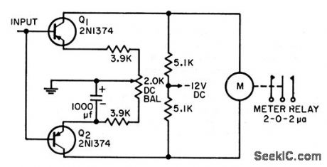
Sensitive and stable d-c amplifier operates relay only on rapid changes of input voltage, yet is immune lo drift. Will also operate on ac signal, which is the some as rapidly changing d-c signal-Rate Circuit, Electronic Circuit Design Handbook, Mactier Pub. Corp. N.Y.1965, p239. (View)
View full Circuit Diagram | Comments | Reading(870)
160_MC_15_W_POWER_AMPLIFIER
Published:2009/7/14 23:25:00 Author:Jessie
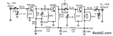
Performance of each of three stages is optimized by using input-output admittance data in network design, to give 30.5 db power gain front class-C operation. Circuit can be expanded to give complete f-m or c-w transmitter by adding appropriate oscillator-buffer-multiplier stages.-R. Hejhall, A 160 MHz 15.Watt Solid-State Power Amplifier, Motorola Application Note AN-214, Nov.1965. (View)
View full Circuit Diagram | Comments | Reading(2275)
2_WATT_POWER_AMPLIFIER_AT_160_MC
Published:2009/7/14 23:08:00 Author:Jessie


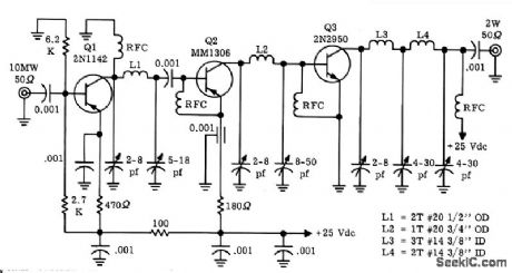
Uses 2N2950 npn silicon planar epitaxial transistor designed for medium-power high-frequency applications. Overall gain is 23 db. Intended for f-m or c-w applications only. For a-m, supply voltage on final stage must be reduced lo 12 v lo remain within voltage rating, and driver should also be 2N2950.-D. L. Adley, Designing 160 Mc FM or CR Circuitry Using a Silicon High Frequency Transistor, Motorola Application Note AN-168, Aug. 1965. (View)
View full Circuit Diagram | Comments | Reading(1116)
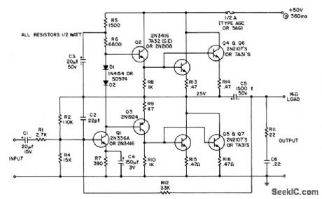
25_W_TRANSFORMERLESS_AMPLIFIER
Published:2009/7/14 23:08:00 Author:Jessie
Uses economical transistors and diodes. Requires 330 mv input for full output. Total harmonic distortion at 1 kc is less than 1% at fulloutput.- Transistor Manual, Seventh Edition, General Electric Co., 1964, p 266. (View)
View full Circuit Diagram | Comments | Reading(982)
HIGH_INPUT_Z_UNITY_GAIN
Published:2009/7/14 20:45:00 Author:May
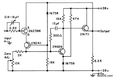
Source-output connection provides feedback. Cascade input stage has high gain, as required for good amplifier gain accuracy. Upper cutoff is 5,000kc for 10,000-ohm generator resistance.-Texas Instruments Inc., Solid-State Communications, McGraw-Hill, N.Y.1966, p141. (View)
View full Circuit Diagram | Comments | Reading(1014)
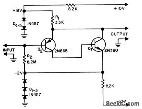
ACTIVE_REDUNDANI_D_C_AMPLIFIER
Published:2009/7/14 20:43:00 Author:May
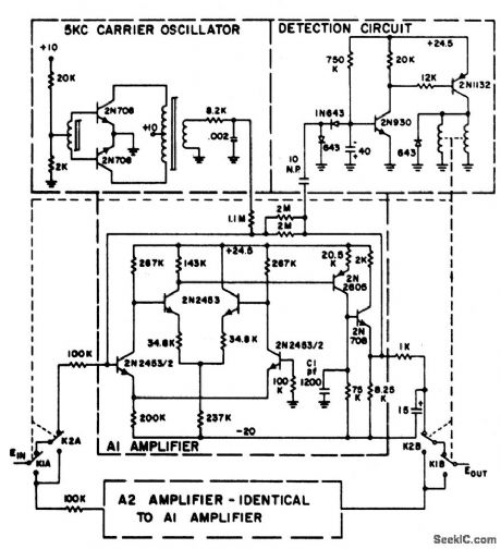
Test carrier signal is added to input of normal amplifier A1. When failure occurs in A1, detector senses absence of test catt'1et and causes relay K to change over to amplifier A2. Both amplifiers ore differential type, having open-loop gain of1,000 and closed-loop gain of 10. Open-loop response is flat to about 2kc, and closed-loop response ex tends beyond 5 kc.-T. B. Hooker, Designing Redundant Analog Amplifiers, EEE, 13:2, p 55-59. (View)
View full Circuit Diagram | Comments | Reading(895)
| Pages:68/250 At 206162636465666768697071727374757677787980Under 20 |
Circuit Categories
power supply circuit
Amplifier Circuit
Basic Circuit
LED and Light Circuit
Sensor Circuit
Signal Processing
Electrical Equipment Circuit
Control Circuit
Remote Control Circuit
A/D-D/A Converter Circuit
Audio Circuit
Measuring and Test Circuit
Communication Circuit
Computer-Related Circuit
555 Circuit
Automotive Circuit
Repairing Circuit