
Amplifier Circuit
Index 77
TRIGGERED_SQUARE_WAVE_GENERATOR
Published:2009/7/16 3:39:00 Author:Jessie
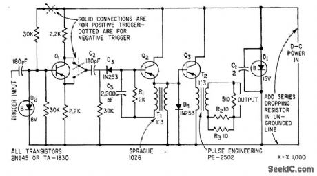
Synchronizing trigger signal drives phase splitter Q1, which in turn feeds blocking oscillator Q2. Output from emitter-follower Q3 is 1-microsec-wide pulse into 90-ohm load. Depending on connections for Q1, either positive or negative input pulse greater than 5 v will trigger generator. Maximum prr is 40 kc.-R. E. Daniels and C. Swoboda, Pulse Generator for Synchronizing Events, Electronics, 33:24, p 63. (View)
View full Circuit Diagram | Comments | Reading(1265)
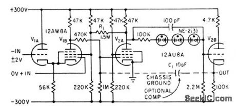
DARLINGTON_INPUT_OPERAIIONAL_AMPLIFIER
Published:2009/7/16 3:38:00 Author:Jessie
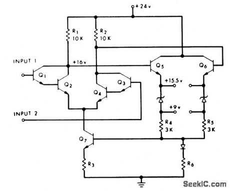
Single-stage version uses emitter-follower output to lower impedance and shift d-c level of output. Q7 and R3 form constant-current source. Zeners, formed as base-emitter junctions of transistors, shift d-c level of outputs negative by 6 V to make them compatible with input voltages and permit cascading of monolithic integrated circuits directly.-C. L. Heizman and D. G. Paterson, Circuit Analysis: A Monolithic Integrated Operational Amplifier, EEE, 13:5, p 80-84. (View)
View full Circuit Diagram | Comments | Reading(979)
THREE_OUTPUT_PRF_GENERATOR
Published:2009/7/16 3:36:00 Author:Jessie
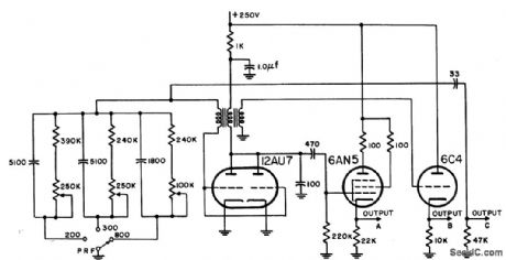
Switch gives choice of 200, 300, and 800 pps. Output C is negative, and other outputs are positive. Output B has positive overshoot to provide trigger that is delayed with respect to out-puts A and C by width of pulse.-NBS, Handbook Preferred Circuits Navy Aeronautical Electronic Equipment, Vol. l, Electron Tube Circuits, 1963, p N5-2. (View)
View full Circuit Diagram | Comments | Reading(906)
AVALANCHE_SWITCH
Published:2009/7/16 3:35:00 Author:Jessie
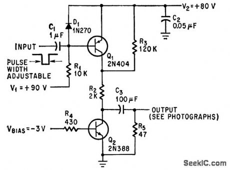
Low-cost germanium transistors used in avalanche mode provide narrow pulses with fast rise times. Width of input pulse determines number of output pulses. For testing counter, collector voltage of Q2 was adjusted for ten pulses per input pulse, at input repetition rate of up to 100,000 pps.-B. S. Ahn, Germanium Transislor As Avalanche Switch, Electronics, 37:30, p 44. (View)
View full Circuit Diagram | Comments | Reading(1074)
SENSE_AMPLIFIER
Published:2009/7/16 3:33:00 Author:Jessie
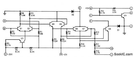
General-purpose amplifier can be used with most coincident-current memories without redesign. Has adjustable threshold, good noise rejection, and drives any standard logic gate with positive or negative output. Bandwidth is 10 Mc. Drift is only 22 microvolts per ℃. Circuit is differential amplifier whose inputs are connected to opposite ends of sense winding. Input accepts both polarities, but output is always same polarity. For negative output pulse, connect F to G; for positive output, connect E to G.-B. Johnson, Sense Amplifier Fis Any Memory, Electronics, 39:18, p 9-94. (View)
View full Circuit Diagram | Comments | Reading(0)
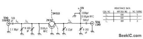
WIDEBAND_ANALOG_AMPLIFIER
Published:2009/7/16 3:32:00 Author:Jessie
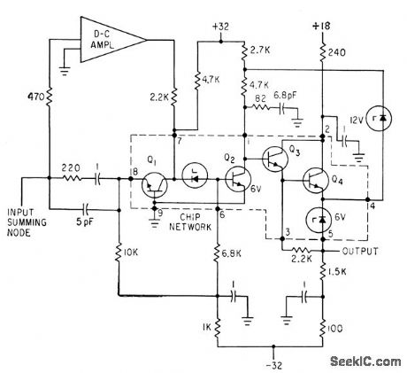
D-C input summing mode signals are amplified in low-drift d-c amplifier and reinserted info amplifier signal path at input to common-emitter stage. Response of d-c amplifier in parallel with common-base stage is complementary to high-frequency amplifier Q2-Q3-Q4, maintaining unit slope down to 1 kc, where gain is 100 db. Loop delay is less than 0.1 nsec. -F. D. Waldhauer, Latest Approach to Integrated Amplifier Design, Electronics, 36:22, p 24-27. (View)
View full Circuit Diagram | Comments | Reading(980)
46_CPS_AMPLIFIER_WITH_8_CPS_BANDPASS
Published:2009/7/16 3:28:00 Author:Jessie
Uses differential input amplifier Q1-Q2 as part of four-stage direct-coupled front end of optically chopped radiometer. Parallel-T filter provides desired frequency characteristic and d-c path for negative feedback around direct-coupled amplifier.-F. Schwarz, Infrared Circuits in Tiros Satellites, Electronics, 34:38, p 43-45. (View)
View full Circuit Diagram | Comments | Reading(762)
50_MC_POWER_AMPLIFIER
Published:2009/7/13 4:35:00 Author:May
Power output is up to 1 w and collector efficiency above 50% for common-base operation.-Texas Instruments Inc., Solid-State Communications, McGraw-Hill, N.Y., 1966, p 317. (View)
View full Circuit Diagram | Comments | Reading(834)
ADJUSTABLE_BANDWIDTH_AMPLIFIER
Published:2009/7/13 4:35:00 Author:May

Bandwidth can be varied from 190 to 280 kc by varying bias voltage on varicap diodes between 0 and 10 v.Used in frequency-response equalization and other system applications requiring automatically adiustable bandwidth in low-poss circuit.-M. G. Wilson, Low-pass Amplifier with Adiustable Bandwidth, Electronics, 39:11, p 90-91. (View)
View full Circuit Diagram | Comments | Reading(768)
250_MC_POWER_AMPUFIER
Published:2009/7/13 4:33:00 Author:May
Gives good per formance for both small and large signals.-Texas Instruments Inc., Solid-State Communications, McGraw-Hill, N.Y., 1966, p 320. (View)
View full Circuit Diagram | Comments | Reading(686)
50_KC_OPERATIONAL_AMPLIFIER
Published:2009/7/13 4:25:00 Author:May

Develops full rated output of 100 v into 10,000-ohm load up to 50 kc. Open-loop gain is 36 db.-H. Koerner, How to Extend Operational Amplifier Response, Electronics, 33:46, p 90-91. (View)
View full Circuit Diagram | Comments | Reading(780)
16_KC_COMPENSATED_OPERATIONAL_AMPLIFIER
Published:2009/7/13 4:24:00 Author:May
Uses pentode V2A as voltage amplifier to provide up to 140 v peak signals at grid of output cathode follower V2A. Will go up to 50 kc without compensation,-H. Koerner, How to Extend Operational Amplifier Response/Electronics, 33:46, p 90-91. (View)
View full Circuit Diagram | Comments | Reading(675)
4_W_WIDE_BAND_AMPLIFIER
Published:2009/7/13 4:20:00 Author:May
Uses complementary transistors for operation up to 100 kc with low distortion. Output is class B.All leads should be kept shott, to minimize tendency to oscillate.-N. Freyling, A 4-Watt Wide-Bond Solid-State Amplifier, Motorola Application Note AN-209, Mar.1966. (View)
View full Circuit Diagram | Comments | Reading(894)
PASSIVE_REDUNDANCY_IN_A_C_AMPLIFIER
Published:2009/7/13 4:17:00 Author:May
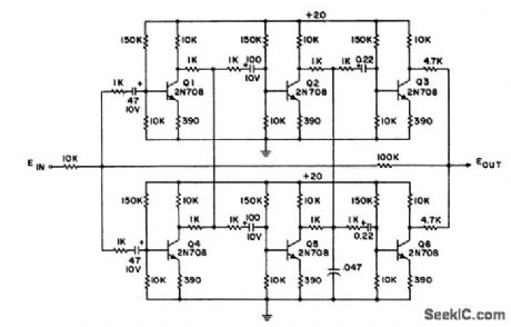
Uses two amplilers connected in parallel on individuol-stage basis, with 1K isolation resistors between stages. Amplifier is operational type having closed-loop gain of 10, open-loop gain of 1,000, and 3-db open-loop frequency response from 30 to 1,500 cps.Both open-loop gain and frequeney response are functions of failure mode of circuit, with most types of failure affecting performance only slightly.-T. B. Booker, Designing Redundant Analog Amplifiers, EEE, 13:2, p 55-59. (View)
View full Circuit Diagram | Comments | Reading(996)
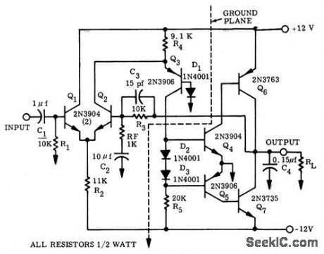
DIODE_STABILIZED_BIAS
Published:2009/7/13 4:16:00 Author:May
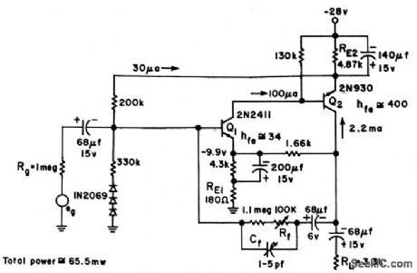
Posilive shunt feedback cancels shunt impedance of bitts network and transistor. RE1 is made small to obtain gain of 10; as a result, input impedance is limited to 1.5 meg. Excellent bias stability is obtained. Three diodes compensate for variations in base-emitter voltage of Q1, and negative d.c feedback from RE2 further increases bias stability. Response is flat within 3 db from 100 cps to 500 kc.-Toxas Instruments Inc., Solid-Stale Communications, McGraw-Hill, N.Y., 1966, p 184. (View)
View full Circuit Diagram | Comments | Reading(912)
100_DB_AMPLIFIER
Published:2009/7/13 4:08:00 Author:May
Used in distortion monitor to drive indicating vtvm.-G. H. Smith, Distortion Monitor Checks Linear Amplifier Characteristics, Electronics, 34:27, p 57-59.
(View)
View full Circuit Diagram | Comments | Reading(769)
PREFERRED_EMITTER_FOLLOWER
Published:2009/7/13 4:07:00 Author:May
Used fo match high-impedance drcuit to low-impedance load. Will accept positive and negative pulses or sinusoidal input. Low output impedance for pulses resuhs in high operating speed into capadtive loads. Bandwidth for 600-ohm source impedonce is 50 cps to 3.5 iAc. Vohctge amplification is 0.8 ond power gain is 12 db.-NBS, Handbook Preferred Circuits Ncvy Aeronautical Electronic Equipment, Vol. II, Semiconductor Device Circuils, 1962, PSC 22 (originally PC 222), p 22-2. (View)
View full Circuit Diagram | Comments | Reading(990)
HIGH_INPUT_Z_FET_AMPLIFIER
Published:2009/7/13 4:06:00 Author:May
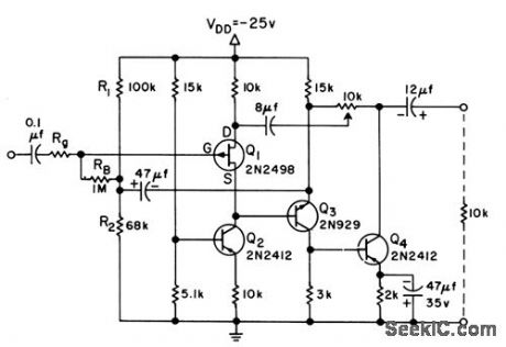
Bias current is obtained from common-base current gen ercttor Q2. Q3 and Q4 function as complementary current multiplier. Bootstrapping for RB is obtained directly from emitter of Q3.Voltage gain is 2 and input impedance is 200 meg. Response is flat within 3 db from 1 to 500 kc with generator resistance of 1 meg.-Texas Instruments Inc., Solid-State Communications, McGraw-Hill,N.Y., 1966, p 187. (View)
View full Circuit Diagram | Comments | Reading(982)
HIGH_IMPEDANCE_PARAMETRIC_AMPLIFIER
Published:2009/7/13 4:05:00 Author:May
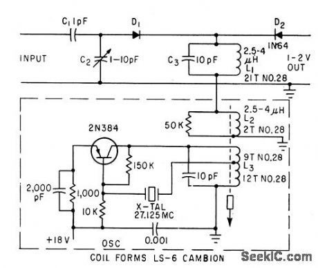
Wide-band amplifier uses diode biased with r-f to give 40-db gain. Input impedance is above 10 gigohms, and frequency response is within 3 db from 3 cps to 200 kc. Diode D1 is energy storage element. Crystal-controlled transistor oscillator is pump frequency source.-D. Rovefi, Diode Amplifer Has Ten.Gigohm Input Impedance, Electronics, 34:51, p 38-40. (View)
View full Circuit Diagram | Comments | Reading(1415)
PLATE_CATHODE_FOLLOWER
Published:2009/7/13 4:03:00 Author:May
Has low output impedance, good gain stability, wide response, and low distortion, making it ideal as bridge driver for Wien-bridge oscillator.-K. H. Liu, Plate-Cathode Follower Wien-Bridge Oscillator, EEE, 11:2, p 27. (View)
View full Circuit Diagram | Comments | Reading(925)
| Pages:77/250 At 206162636465666768697071727374757677787980Under 20 |
Circuit Categories
power supply circuit
Amplifier Circuit
Basic Circuit
LED and Light Circuit
Sensor Circuit
Signal Processing
Electrical Equipment Circuit
Control Circuit
Remote Control Circuit
A/D-D/A Converter Circuit
Audio Circuit
Measuring and Test Circuit
Communication Circuit
Computer-Related Circuit
555 Circuit
Automotive Circuit
Repairing Circuit