
Amplifier Circuit
Index 79
RECEIVER_RF_PREAMP
Published:2009/7/13 2:46:00 Author:May
The RF broadband preamplifier uses an NPN VHF transistor as an untuned broadband (0.5 to 30 MHz) RF amplifier. Input impedance is 50Ω, allowing usage for all receiver inputs, and the unit has a 600-Ω output to match virtually all RF input circuits. The preamp delivers 30 dB of gain at 10 MHz, with a noise factor below 1 dB. Power for the preamp can be obtained from a variety of sources. The assembly requires from 9 to 14 Vdc and draws 8 mA of current. This makes it ideal for use in battery-operated portable equipment. (View)
View full Circuit Diagram | Comments | Reading(2907)
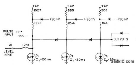
OPEN_FUSE_DETECTOR
Published:2009/7/16 5:22:00 Author:Jessie
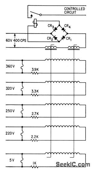
Magamp circuit uses bridge unbalance to operate control relay when protective fuse opens in digital com puter, to remove d-c voltages from fused section. One of 15 control windings of series-connected magnetic amplifier is placed across each fuse, with appropriate current-limiting resistor in series with each winding. (Only representative control windings are shown)-J. Maroz, Magnetic Amplifier Detects Open Fuses, Electronics, 31:29, p 86-92. (View)
View full Circuit Diagram | Comments | Reading(929)
THREE_STAGE_MAGNETIC_SERVO
Published:2009/7/16 5:19:00 Author:Jessie
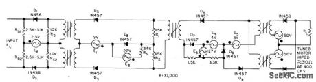
Has balanced two-core input, alternate-firing output stage, and synchronous interstage switches to eliminate interaction between stages.Power gain approaches 60 db. Zero drift is less than 0.25 deg, accuracy is within 0.5deg, and follow-up rate is 300 deg per sec.-C. C. Voice, Magnetic Amplifier Drives Gyro Indicator, Electronics, 31:7, p 114-117. (View)
View full Circuit Diagram | Comments | Reading(839)
MAGNETIC_AMPLIFIER
Published:2009/7/16 5:18:00 Author:Jessie
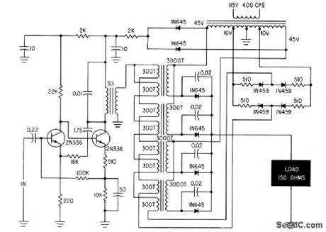
Used in aircraft fuel low indicating system. Transistor preamp has stabilized gain of 350.-E. Van Winkle, A-C Controlled Half-Cycle Magnetic Ampli-0er, Electronics, 34:15, p 75-77. (View)
View full Circuit Diagram | Comments | Reading(1318)
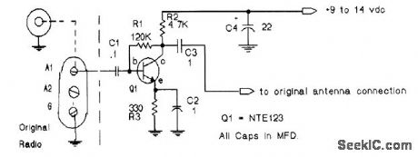
RECEIVER_PREAMPLIFIER
Published:2009/7/13 2:45:00 Author:May

This preamplifier lets you use a short antenna over the range from 100 kHz to well over 55 MHz, with excellent sensitivity, using a vertical 30-in piece of #12 wire or a few feet of wire laying on the floor. Transistor Q1 (NPN) is directly coupled to PNP transistor Q2. Feedback from the collector of Q2 to the emitter of Q1 is accomplished by resistors RF and RA. Because of the high open-loop gain of the amplifier, the gain of the amplifier is RF/RA, or 20 dB maximum. A 1-kΩ potentiometer changes the effective value of RA resulting in a minimum gain of near unity. (View)
View full Circuit Diagram | Comments | Reading(1262)
LOW_NOISE_9_MHz_AGC_CONTROLLED_AMPLIFIER
Published:2009/7/13 2:44:00 Author:May

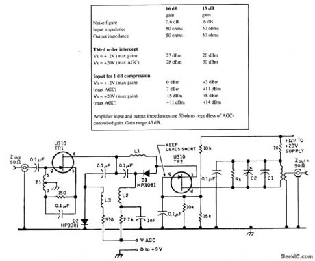
The circuit diagram of the 9-MHz amplifier is given. Note that the AGC amplifier must be capable of sinking the current through D1 at 0 V (i.e., maximum gain). The warning to keep leads short in the drain circuit of the second U310 FET arises from experience in which the initial IP3 measurements proved to be poor because of this stage's oscillating around 400 MHz.Component notes: The two U310s are Siliconix low-noise JFETs. C1 is an 82-pF ceramic, C2 is a 60-pF ceramic trimmer (Cirkit), and all other capacitors are monolithic ceramic (RS components). Resistors are l/8 Wmetalfilm (RS components). D1 and D2 are HP3081 PIN diodes (Farnell). T1 is 1518 turns of 0.224-mm diameter Bicelflux enamel on Fairite Balun core 28-43002402 (Cirkit). T2 (primary) is 2.81 μH, 31 turns of 0.314-mm Bicelflux enamel on Micrometals toroid 737-6 (Cirkit). T2 (secondary) is (1) for 16-dB gain, 3 turns, Rx 6k2; (2) for 13-dB gain, 4 turns, Rx 3k9. Note that (1) and (2) could be relay switched for use with an SSB or CW filter (loss 10 dB or 3 dB). L1, L2, and L3 have 7 turns of 9.314-mm enamel on balun core 28-43002402 (Cirkit). (View)
View full Circuit Diagram | Comments | Reading(1979)
Y_AMPLIFIER_FOR_COINCIDENI_FLUX_MEM_ORY
Published:2009/7/16 5:11:00 Author:Jessie
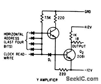
Inputs to translator section of Y amplifier are last four bits of address, which perform one out of ten translations for horizontal matrix of 1,120-bit memory.-H. F.Priebe, Jr., Three-Hole Cores for Coincident-Flux Memory, Electronics, 33;31, p 94-97. (View)
View full Circuit Diagram | Comments | Reading(849)
GENERAL-PURPOSE_WIDEBAND_PREAMP
Published:2009/7/13 2:42:00 Author:May
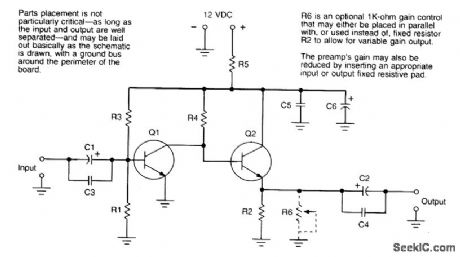
This preamp has a galn of35 dB at 100 kHz,30 dB at 10 MHz,and 17 dB at 100 MHz and draws 15 mA at 12 V. (View)
View full Circuit Diagram | Comments | Reading(1035)
BIDIRECTIONAL_PF_AMPLIFIER
Published:2009/7/13 2:41:00 Author:May
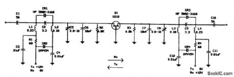
JFETS can often be used with the source and drain interchanged. This interesting circuit makes use of this fact as a bidirectional RE amplifier at 70.0455 MHz. It is useful for transceiver applications. (View)
View full Circuit Diagram | Comments | Reading(1158)
25_W_SOLID_STATE_LINEAR_AMPLIFIER
Published:2009/7/13 2:39:00 Author:May
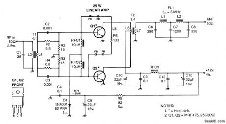
This shows a schematic diagram of the 25-W linear amplifier. Decimal-value capacitors are in microfarads; others are in picofarads. Polarized capacitors are electrolytic or tantalum, 16 V or greater. Resistors other than R5 are 1/4-W carbon-composition or carbon-film units. (View)
View full Circuit Diagram | Comments | Reading(2770)
TUNNEL_DIODE_AND_GATE
Published:2009/7/16 5:03:00 Author:Jessie
Three cascaded monostable multivibrators provide required gain at 200 Mc.-E. Gottlieb and J. Giorgis, Tunnel-Diode Switching Circuits, Electronics, 36:27, p 26-31. (View)
View full Circuit Diagram | Comments | Reading(0)
1930~1990MHz narrowband linear amplification circuit composed of RF2320
Published:2011/8/4 5:00:00 Author:May | Keyword: narrowband linear amplification
The picture shows 1930~1990MHz narrowband linear amplification circuit composed of RF2320. Radio-frequency signal (RF) is input by pin 6. Then it is output by pin 14 after passing amplifier. Pin 6 is direct coupled with internal amplifier. So it adds a blocking coupling capacitor. Normally, the gate voltage of input end is 0V. But the gate voltage will be enlarged when extent bias enlarges, and current will be increased at the same time. But it can not improve the linearity of amplifier. Pin 14 provides output and internal bias. There is no blocking coupling capacitor in the chip, but this pin has DC voltage. So it adopts 22pF capacitor to use as blocking capacitor. In order to get thelargest output power and efficiency, output matching network can make output impedance of amplifier match with it.
(View)
View full Circuit Diagram | Comments | Reading(788)
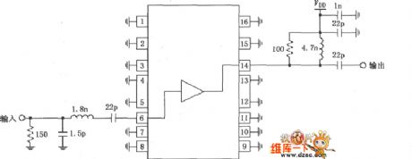
1.8_to_72_MHz_POWER_AMPLIFIER
Published:2009/7/13 2:38:00 Author:May

A novel approach to a 250-W power amplifier (PA) is shown. The driver uses a pair of low-cost ICs, rather than the conventional RF transformer to provide out-of-phase driving signals for the two final MOSFETs. It also provides hard limiting (sine -wave-to-square -wave conversion) of the input signal. The Elantec EL7144C is intended for use as a gate driver. The internal Schmidt trigger allows it to serve as a hard limiter, and the presence of both inverting and noninverting inputs allows a pair to serve as a phase splitter. The RF input is ac-coupled to the noninverting input of U1 and the inverting input of U2. Adjustment of the biases via R6 and R8 allows the transition points to be selected to produce the desired duty ratio (50:50). The phase error between the two EL7144s is about 0.5 ns. (If an oscilloscope is not available, use a voltmeter with a 1-kΩ series resistor and setthe average output voltage to 6 V.) The EL7144s have high input impedances, so R5 provides a 50-V input impedance for the signal source. Input signals in the range of 10 to 100 mW are satisfactory, allowing this PA to be driven directly from a laboratory signal generator or oscillator with buffer.The best switching speed is obtained with VDD1=12 V. Output transistors are ARF440 and ARF441.See parts list. (View)
View full Circuit Diagram | Comments | Reading(1887)
POS CDMA/TDMA PA driver amplifier FR2324 pin data
Published:2011/8/4 2:46:00 Author:May | Keyword: driver amplifier
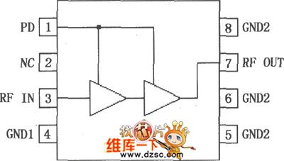
RF2324 is CDMA/TDMAPA driver amplifier with very large dynamic range. It is designedfor 1800MHz emission digital PCS signal.The device is used as aPA driver amplifier with outstanding properties, it can solve the low emission noise power problem which is cared by digital user. RF2324 has the property of power down control ,and itcan total close the device. RF2324 adopts standard small 8 pins MSOP plastic package. Its pin array is shown in the diagram.
The pin function is shown in the follwing diagram
(View)
View full Circuit Diagram | Comments | Reading(805)
STEREO_AUDIO_COMPRESSOR
Published:2009/7/13 2:28:00 Author:May
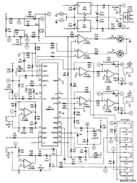
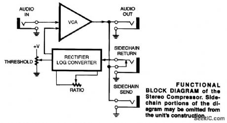

The block diagram of the stereo compressor is shown. The input signal is fed to a voltage-con-trolled amplifier (VCA) that has a nominal gain of unity. Some of the output signal is fed to a precision rectifier followed by a logarithmic converter circuit. The output of this block is a dc voltage proportional to the log of the average level of the input signal. By sending some of this dc control voltage to the VCA, the gain of the VCA is automatically reduced when the input signal exceeds a user-determined threshold level. It is important to note that the signal level is determined after the VCA and not before. This allows the output level to increase and sound normal, but not increase as much as the input signal does. By varying the amount of feedback, the compression ratio is adjusted, which, in conjunction with the THRESHOLD control, determines the operating characteristics of the compressor. The optional sidechain jacks permit external processing of the audio signal or substitution of a completely different audio signal as the control signal. This add-on circuitry lets the user ex-periment and achieve some useful audio effects. (View)
View full Circuit Diagram | Comments | Reading(3125)
CURRENT_DIFFERENCE_AMPLIFIER
Published:2009/7/13 2:14:00 Author:May
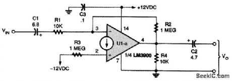
This practical 20-dB gam ac amplifier uses the LM3900 CDA. (View)
View full Circuit Diagram | Comments | Reading(799)
LM3900_AC_AMPLIFIER
Published:2009/7/13 2:12:00 Author:May
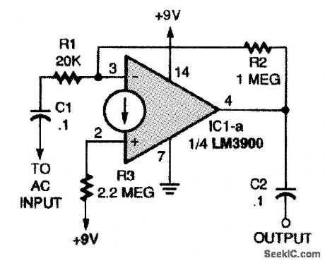
Although the LM3900 current difference amplifier (IC1) used in this ac amplifier really isn't a true op amp, it does simulate one in its performance; however, the IC requires only a one-polarity power source.Gain is R2/R1, and R3 is 2×R2. (View)
View full Circuit Diagram | Comments | Reading(1827)
CLAMP_AMPLIFIER
Published:2009/7/13 2:11:00 Author:May
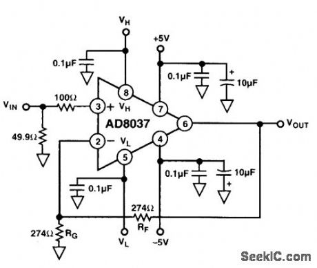
A clamp amplifier is a limiting or bounding circuit. For input voltages between two levels, VH and VL, the output is proportional to the input. For inputs greater than VH or less than VL (VH or VL × the amplifier gain, AV), irrespective of the input. The threshold voltages, VH and VL, can be fixed or variable. If the amplifier can handle positive and negative input/output voltages, VH and VL can have any positive or negative value within the specified range, as long as VH > VL. (View)
View full Circuit Diagram | Comments | Reading(997)
PROGRAMMABLE_AMPLIFIER
Published:2009/7/13 2:07:00 Author:May
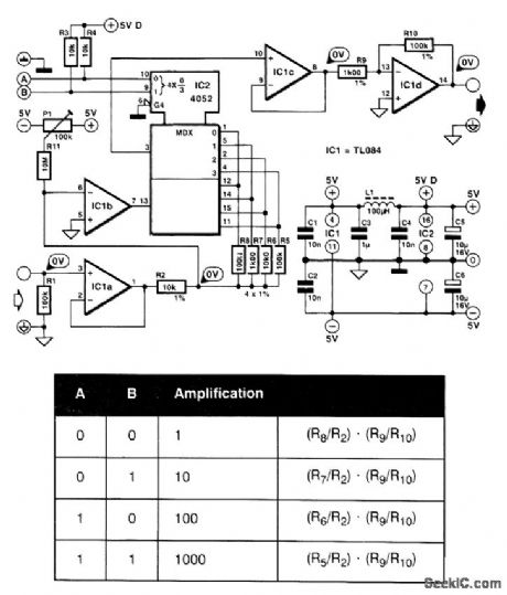
The programmable gain amplifier (PGA) is ideal for applications, such as data loggers and automatic measuring instruments. The amplification can be set anywhere between unity and ×1000. The bandwidth at any amplification is >30 kHz. The current drain does not exceed 7 mA. The input signal is buffered by IC1a and then applied to amplifier IC1b. The amplification of this stage depends on how feedback resistors R5 to R8 are switched into the circuit by IC2. How the resistors are inter-coupled depends on the logic levels at inputs A and B. The interrelation among the resistors, the total amplification, and the logic levels is shown in the table. After the output signal of IC1b has passed through the multiplexer, it is applied at ×100 amplifier IC1d via buffer IC1c. The overall amplification is set with logic levels at inputs A and B as shown in the table. The amplification of the first stage has been kept low purposely to ensure that the value of the feedback resistor does not have to be high, which makes the effect of the leakage current of the multiplexer negligible. (View)
View full Circuit Diagram | Comments | Reading(0)
COMPRESSION_AMPLIFIER
Published:2009/7/13 2:04:00 Author:May
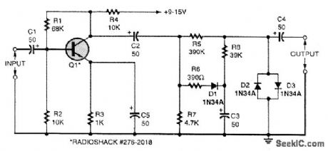
Here's a compression-type amplifier that can be used to keep the volume level of an organ constant. Unlike compressors used for public-addr ess-system applications, the organ leveler can respond to the entire range of frequencies generated by the organ without-coloring the voice. It can handle large fluctuations in input signal without clippinl. It also works well as a microphone leveler (View)
View full Circuit Diagram | Comments | Reading(2327)
| Pages:79/250 At 206162636465666768697071727374757677787980Under 20 |
Circuit Categories
power supply circuit
Amplifier Circuit
Basic Circuit
LED and Light Circuit
Sensor Circuit
Signal Processing
Electrical Equipment Circuit
Control Circuit
Remote Control Circuit
A/D-D/A Converter Circuit
Audio Circuit
Measuring and Test Circuit
Communication Circuit
Computer-Related Circuit
555 Circuit
Automotive Circuit
Repairing Circuit