
Amplifier Circuit
Index 67
Op amp zero method circuit diagram
Published:2011/8/4 20:55:00 Author:Rebekka | Keyword: Op amp, zero method
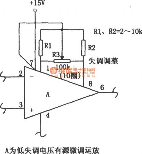
The high-resolution zero circuit is shown as above. It can adjust the 100 ~ 200μV offset voltage to l ~ 2μV. R3 in the circuit isthe high multi-turn ceramic trimmer potentiometer with high resistance. The potentiometeris connected tothe internal resistor of amplifier(typically around 1 ~ 10kΩ) in parallel.Resistors R. And R: They are the l% precision metal film resistors,which can provide the required resolution and range. The resistance range is 2 ~ 10MΩ. For some integrated operational amplifiers,it doesn't need external R1 and R2 to minimize the noise. (View)
View full Circuit Diagram | Comments | Reading(781)
CFl4753 single and dual power high input impedance quad op amp circuit diagram
Published:2011/8/4 20:58:00 Author:Rebekka | Keyword: high input impedance, single power , quad op amp, dual power
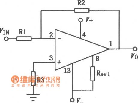
CF14753 is CMOS operational amplifier, containing 4 units high-performance op amp。 It is exactly the same with foreign model MC14753. It isset internal phase compensation and mainly used for a variety of analog computing circuits, AC amplifier, low-frequency waveform generator and the active filter. It also can be composed of chopping and auto-zero operational amplifier. Its similar or direct substitutions models are: CFl4573, 5G14573, MCl4573, CHl4573, CAl4573 and so on. The typical application circuit is shown as above. (View)
View full Circuit Diagram | Comments | Reading(705)
High-precision linear amplifier circuit composed of F007
Published:2011/8/4 20:59:00 Author:Rebekka | Keyword: linear amplifier
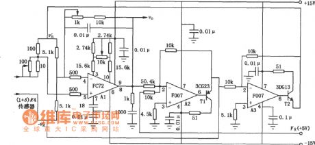
High-precision linear amplifier circuit is used for sensing signal detection. It is shown as above. The high-precision linear amplifier circuit is composed of three parts, electric bridge, op amp amplifiers Al and supply amplifier A2 and A3. The output value of A2 and A3 are equal, the phases are contrast, its size depends on the reference voltage VR and the output voltage Vo. The (1 + δ)R4 in the bridge shows the resistance change value of the temperature sensor. The linear distortion of the circuit is not more than 0.5%, it can be used for the temperature measurement interface of the air data processing system, it can be used as the non-power measurement of pressure, speed, flow etc. (View)
View full Circuit Diagram | Comments | Reading(1239)
BTL power amplifier circuit compoed of LF4100
Published:2011/8/4 20:46:00 Author:Rebekka | Keyword: BTL power amplifier
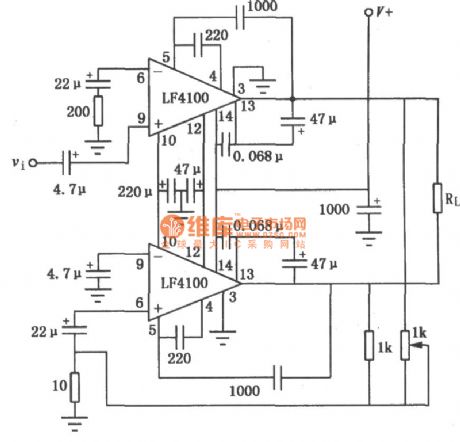
LF4100, 4101 and 4102 are mainly used for tape recorders, amplifiers and other electronic equipment of audio power amplifier. The device has a wide frequency response, high fidelity, high stability and the feature of easy to adjust stc. BTL power amplifier circuit composed of LF4100, 4101 and 4102 is shown as above. (View)
View full Circuit Diagram | Comments | Reading(870)
Isolated electric bridge measurement amplifier circuit composed of INA102
Published:2011/8/4 20:50:00 Author:Rebekka | Keyword: Isolated electric bridge , measurement amplifier
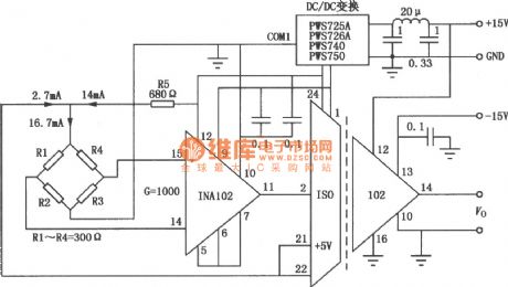
The isolated electric bridge measurement amplifier circuit is composed of ISO102 and low-noise low-power INA102, whichis widely used in industrial process control, andit is shown as above. ISO102 is the buffer capacitor coupled isolation amplifier, the gain of the INA102 is 1000,and itmain amplifies 300Ωbridge signal. Bridge power supply is composed of two parts: One part is l4mA current provided by the supply side (INA102 12 feet) passing the 680Ω resistor; Another part is 2.7mA current provided by the +5 V reference from the ISO102 incentive. The 2 parts supply 16.7mA to the electric bridge. (View)
View full Circuit Diagram | Comments | Reading(766)
Gain Programmable Amplification Circuit Composed Of OPA676
Published:2011/8/4 20:52:00 Author:Robert | Keyword: Gain, Programmable, Amplification
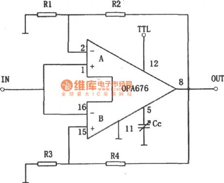
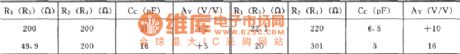


The picture shows the gain programmable amplification circuit. This circuit is mainly made up of OPA676 integrated chip. And the OPA676's internal part has two channels amplification circuit which is marked as A channel and B channel separately (see the A and B in the picture). The two channels' conducting mode or not conducting mode are controlled by the pin 12's voltage level (which is called TTL port). If the TTL port's voltage is high level, the A channel (the higher part of the circuit) would work and the B channel (the lower part of the circuit ) would be not conducted. Otherwise when the TTL port is in low voltage level, the A channel would be not conducted and the B channel would work. The A channel's voltage magnification is AVA=1+R4/R3, and the B channel's voltage magnification is AVB=1+R4/R3. So it could only select different R1, R2 or R3, R4, the A and B channels would have different gain. By controlling the A and B channels selection port TTL's voltage level (pin 12), it could be easy to achieve the gain programmable control. (View)
View full Circuit Diagram | Comments | Reading(769)
MONITOR_VIDEO_AMPLIFIER
Published:2009/7/14 21:52:00 Author:Jessie
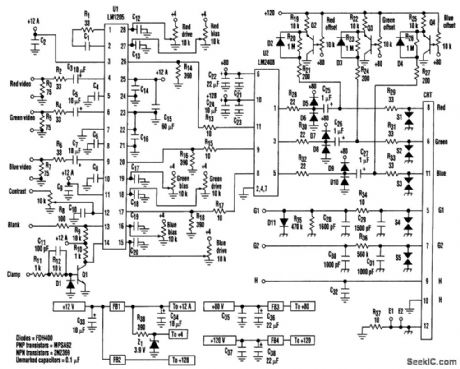
This circuit uses a preamplifier and a video driver IC The monitor video amplifier will affect all aspects of future computer monitors,including higher-resolution pictures and faster video speeds,Such an amplifier is usually split into a preamplifier section and a CRT driver section (View)
View full Circuit Diagram | Comments | Reading(2536)
COMPLEMENTARY_SYMMEIRY_AUDIO_AMPLIFIER
Published:2009/7/14 22:14:00 Author:Jessie
Provides nearly maximum power theoreticallyavailable from single d-c supply.Distortion is low,large feedbacks, both a-c and d-c, make amplifier insensitive to unbalance of output transistors.-R. S. Richards, How to Design Transformerless Audio-Frequency Power Amplifers, Electronics, 35:46, p 50-52. (View)
View full Circuit Diagram | Comments | Reading(1072)
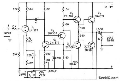
VIDEO_AMPLIFIER_WITH_SYNC_STRIPPER_AND_DC_RESTORER
Published:2009/7/14 22:11:00 Author:Jessie
This circuit transmits 220-MHz (-3-dB bandwidth) video signals while stripping off the sync pulse and performing dc restoration. It is configured for a typical video cable-driver application driving a double-terminated 75-Ω load. In other words, the HFA1103 (IC3) is configured for a gain of +2 to ensure unity gain overall. The HFA1103 video op amp is specially designed to perform sync stripping. Its open-emitter NPN output forms an emitter-follower with the load resistor, and passes the active video signal while virtually eliminating the negative sync pulse. Residual sync, defined as the remainder of the original -300-mV sync pulse, referenced to ground, is only 8 mV at the cable output of the HFA1103. Because the HFA1103 contains no active pull-down, output linearity degrades as the signal approaches 0 V. To deal with this, a 6.8-kΩ pull-up resistor (R8) and a 75-Ω pull-down resistor (R10) on the output ensure a fixed positive offset voltage, in this case, +50 rnV. This offset was arbitrarily chosen as a good compromise between linearity near the dc level and minimum residual sync. Increasing R8 decreases residual sync at the expense of linearity. Conversely, lowering R8, decreases linearity error, but increases residual sync. This circuit achieves dc restoration by using a CA5260 dual op amp (IC1a, IC1b) coupled with a sample-and-hold circuit, based on a 74HC4053 switch (IC2). Vin ,consisting of the input video signal and a dc offset (Vdc) ,is connected to the noninverting input of (View)
View full Circuit Diagram | Comments | Reading(1439)
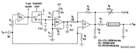
6_V_PHONO_AMPLIFIER
Published:2009/7/14 22:26:00 Author:Jessie
Provides 300 mw at 10% distortion. Bass control R1 and treble control R2 are 50K linear taper. Volume control R3 is 10K audio taper.- Transistor Manual, seventh Edition, General Electric Co.,1964,p 376. (View)
View full Circuit Diagram | Comments | Reading(789)
VIDEO_DISTRIBUTION_AMPLIFIER
Published:2009/7/14 22:26:00 Author:Jessie
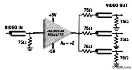
This video distribution amplifier uses a single MAX4278 with a gain of 2 (6 dB) so that three 75-Ω loads can be driven from one 75-Ω source. Each driven load has a source impedance of 75Ω. Gain is flat to 0.1 dB up to 150 MHz. (View)
View full Circuit Diagram | Comments | Reading(4370)
PREFERRED_POWER_AMPLIFIER
Published:2009/7/14 22:23:00 Author:Jessie
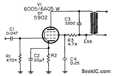
For 6AQ5W, with plate supply of 250 v, output is 115 v to transformer at 2.21 w for 6 v rms input. For 5902, with plate supply of 150 v, output to transformer is 75 v at 0.8 w for 5 v rms input.-NBS, Handbook Preferred Circuits Navy Aeronautical Electronic Equipment, Vol. I, Electron Tube Circuits, 1963, PC 61, p 61-2. (View)
View full Circuit Diagram | Comments | Reading(1690)
PREFERRED_VOLTAGE_AMPLIFIER
Published:2009/7/14 22:31:00 Author:Jessie
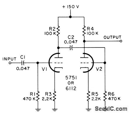
Amplifies 10 to 70-my signals to level needed to driveaudio power amplifier. For 5751, amplification is 335 , maximum output is 23 v rms,and 3-db response is 10 cps to 20 kc. For 6112, maximum output is 26 v rms,amplification is 370, and 3-db bandwidth is 10 cps to 30 kc.-NBS, Handbook Preferred Circuits Navy Aeronautical Electronic Equipment, Vol. I, Electron Tube Circuits, 1963, PC 60, p 60-2. (View)
View full Circuit Diagram | Comments | Reading(1353)
9_V_PHONO_AMPLIFIER
Published:2009/7/14 22:35:00 Author:Jessie
Provides 400 mw at 10% distortion. R1 is 5K audio taper and R2 is 25K linear taper- Transistor Manual, Seventh Edition, General Electric Co.,1964, p 377. (View)
View full Circuit Diagram | Comments | Reading(766)
10_W_DIRECT_COUPLED_POWER_AMPLIFIER
Published:2009/7/14 22:34:00 Author:Jessie


Has excellent low-frequency response, along with d-c feedback for temperature stabilization of all stages. Q2 and Q3 operate dass Bin Darlington connection to increase current gain. Fuses protect output transistorsagainst continuous sine. wave output above 10 kc. Power response at 1 w is fat from 30cps to 15 kc.- Transistor Manual, Seventh Edition, General Electric Co., 1964, p260. (View)
View full Circuit Diagram | Comments | Reading(1335)
STABLE_AUDIO_AMPLIFIER
Published:2009/7/14 22:44:00 Author:Jessie
Provides low input and output impedances, along with stable gain for wide range of transistor parameters and thus for temperature and supply voltage variations, as required for sound level meter.-W. V. Richings and B. J.White, Transistorized Sound Level Meter, Electronics, 33:25, p 64-66. (View)
View full Circuit Diagram | Comments | Reading(980)
TELEPHONE_CHANNEL_AMPLIFIER
Published:2009/7/14 22:41:00 Author:Jessie


Thick film construction gives 36 db gives and is distortion. free up to 65 mw. Input and output impedances are 600 ohms, for frequency multiplex equipment.-N. A Zellmer, Getting the Most out of Feedback,Electronics,39:2, p 66-72. (View)
View full Circuit Diagram | Comments | Reading(730)
HI_FI_FET_PREAMP
Published:2009/7/14 22:39:00 Author:Jessie


Breakdown voltage of commercial fet's is extended by using direct.coupled cascade connection with low-cost germanium transistor.-L. J. Sevin, Jr., Field Effect Transistors, McGraw-Hill, N.Y., 1965, p 73. (View)
View full Circuit Diagram | Comments | Reading(1481)
TUNABLE_ULTRASONIC_AMPLIFIER
Published:2009/7/14 21:20:00 Author:May
The RF portion of the VLF receiver is shown (a precise rectifier/filter circuit is needed following the output of the figure to generate the dc signal monitored by SID hunters). To tune the SID-hunting frequencies, C2 is 0.001μF. The range of inductance simulated is 10.9 to 43.9 MHz. If C1 is a 0.002-μF unit, then the tuning range is 17 to 34 kHz. (View)
View full Circuit Diagram | Comments | Reading(1507)
8_W_SILICON_TRANSISTOR_POWER_AMPLIFIER
Published:2009/7/14 22:48:00 Author:Jessie
Output impedance is 0.5 ohm, for good speaker damping,Response is down only 3 db at 86 kc.Power response is flat Within 0.33 db from 30 cps to 15 kc at 6 w output.- Transistor Manucal, Seventh Edition, General Electric Co., 1964, p 263. (View)
View full Circuit Diagram | Comments | Reading(1338)
| Pages:67/250 At 206162636465666768697071727374757677787980Under 20 |
Circuit Categories
power supply circuit
Amplifier Circuit
Basic Circuit
LED and Light Circuit
Sensor Circuit
Signal Processing
Electrical Equipment Circuit
Control Circuit
Remote Control Circuit
A/D-D/A Converter Circuit
Audio Circuit
Measuring and Test Circuit
Communication Circuit
Computer-Related Circuit
555 Circuit
Automotive Circuit
Repairing Circuit