
Amplifier Circuit
Index 71
CASSETTE_PREAMP
Published:2009/7/14 5:10:00 Author:May
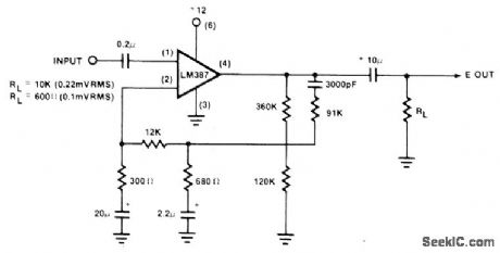
Provides gain of 81 dB and 0.22 mVRMS for 10K load. Gain drops to about 78 dB and output is 0.1 mVBMS for 600-ohm load. Gain values are for 100 Hz, with gain dropping above and below this value.- Signetics Analog Data Manual, Signetics, Sunnyvale, CA, 1977, p 782. (View)
View full Circuit Diagram | Comments | Reading(1201)
CONSTANI_CURRENT_CAPACITOR_CHARGER
Published:2009/7/14 5:08:00 Author:May
Firing angle of a-c supply voltage is decreased in steps after each supply cycle, to match charging rate of 360-mfd capacitor for 30-kw plasma pinch space engine. So current pulses have identical average peak of 8.6 amp.-F. Ellern. Capacitance Chargers for Space Employ Controlled Rectifiers, Electronics.36:41,p32-33 (View)
View full Circuit Diagram | Comments | Reading(942)
FAST_TURN_ON_PLAYBACK_PREAMP
Published:2009/7/14 5:22:00 Author:May
Turn-on for gain and supply voltage is only 0.1 s, as com-pared to 5 s normally required in preamp providing NAB tape playback response.- Audio Handbook, National Semiconductor, Santa Clara, CA, 1977, p 2-31-2-37. (View)
View full Circuit Diagram | Comments | Reading(748)
TIME_AMPLIFIER
Published:2009/7/15 3:18:00 Author:Jessie
Output pulse width is linear function of input pulse width. With two stages, circuit con amplify nanosec pulse widths to seconds. Article gives design procedure for choosing values of R1, C1, and R2 for desired time amplification and input pulse range. For input of 0.1-1 microsec and time amplification of 1,000, R1 = 51, C1 8,200 mfd, and R2 3.2 meg. For 10-100 microsec input and amplification of 100, R1 is increased to 510 ohms For 100 to 1.000 microsec input and amplification of 10, R1 = 510, C1 = 0.82 mfd, and R2 =320K,-R.W.Fergus, Time Amplifier,EEE,11:8, p 26-27. (View)
View full Circuit Diagram | Comments | Reading(982)
REZEROING_AMPLIFIER
Published:2009/7/14 4:55:00 Author:May
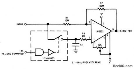
Used where input signal has unknown and variable DG offset, as in telemetry applications. Rezero command line is enabled while ground reference signal is applied to input, making C1 charge to level proportional to DC offset of system. When rezero line is deactivated, amplifier becomes conventional inverter, subtracting system offset and giving true ground-referenced output. For 10-V full-scale system requiring 0.1% (10-mV) accuracy, amplifier needs rezeroing reference every 100 ms.- Linear Applications, Vol. 1, National Semiconductor, Santa Clara, CA, 1973, AN-63, p 1-12. (View)
View full Circuit Diagram | Comments | Reading(764)
SINGLE_STAGE_AUDIO_AMPLIFIER
Published:2009/7/15 2:57:00 Author:Jessie
Design procedure is given for basic transistor stage.- Transistor Manual, Seventh Edition, General Electric Co., 1964, p 241. (View)
View full Circuit Diagram | Comments | Reading(1177)
LINEAR_AMPLIFIER
Published:2009/7/15 3:33:00 Author:Jessie

Motorola MHW-710 power module boosts 1-W output of VHF Engineering TX-432B crystal-controlled solidstate exciter to about 10 W for simple amateur TV transmitter. Interconnections are made with short lengths of FIG-174 coax. Input jack J1 is connected to exciter by 50 ft of RG-174, and length is gradually reduced until proper drive level is obtained for linear operation. RFC uses 8 turns No. 22 enamel on 1-megohm 1-W resistor. To cover 400-440 MHz, use MHW-710-1; for 440-470 MHz, use MHW-710-2.-R. E. Taggart, Interested in Television?, 73 Magazine, Oct. 1977, p 164-174. (View)
View full Circuit Diagram | Comments | Reading(2638)
400_cps_INVERTER_POWER_AMPLIFIER
Published:2009/7/15 3:32:00 Author:Jessie
Has low internal impedance and low distortion, to Provide good output voltage regulation for d-c to 400-cps a-c inverter. Uses com pounded common-collector output stage. Delivers 55 w at 400-cps with only 2.4% total harmonic distortion.. -R. Wileman, Linear Circuits Regulate Solid-state Invertel, Electronics,33:16,p6l-63. (View)
View full Circuit Diagram | Comments | Reading(1247)
HIGH_VOLTAGE_FLASH_PULSER
Published:2009/7/14 4:17:00 Author:May
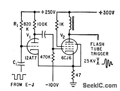
Two identical pulse generators are used to fire two flash tubes alternately lm high-speed strobe. One unit is coupled to each plate of an Eccles-Jordan trigger, to produce required alternating trigger sequence.-L. H. Barrett, New Circuit Improves Stroboscope Versatility, Electronics, 32:32, p 116-118. (View)
View full Circuit Diagram | Comments | Reading(877)
1_WATT_FET_AUDIO_AMPUFIER
Published:2009/7/14 4:13:00 Author:May

Voltage amplifier is followed by split-load phase inverter and push-pull output stage. Emitter-followers drive output stage to improve transistors, McGraw-Hill, N.Y., 1965, p 98. (View)
View full Circuit Diagram | Comments | Reading(929)
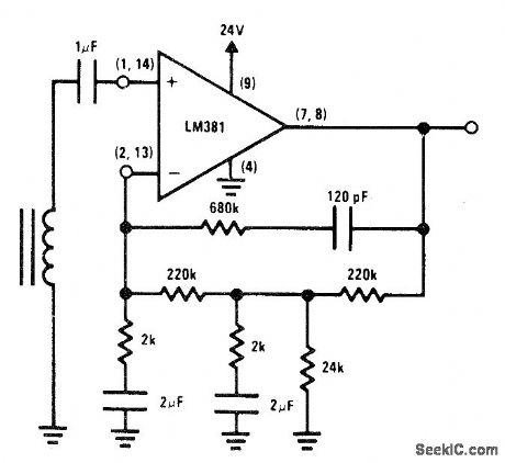
PHONO_PREAMP_1
Published:2009/7/14 4:11:00 Author:May


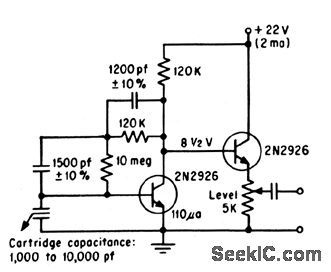
Two planar passivated silicon transistors give RIAA equalization for ceramic cartridge.-General Electric Co.(ad),Electronics, 37:17, p 38. (View)
View full Circuit Diagram | Comments | Reading(1096)
40_METER_35_W_AMPLIFIER
Published:2009/7/14 4:10:00 Author:May
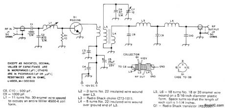
Designed for use with low-power(QRP)transmitter when band conditions are poor. Requires about 350-mW input. Half-wave filter at output keeps harmonics low Use heatsink for Q1.-T Mula, Codzila 1, QST, Feb. 1977, p14 – 15. (View)
View full Circuit Diagram | Comments | Reading(1118)
METER_AMPLIFIER
Published:2009/7/15 4:48:00 Author:Jessie
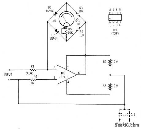
Meter in feedback path of opamp is connected in bridge circuit for measuring both AC and DC voltages. Input voltage is equal to meter current in amperes multiplied by 3 times value of R1 in ohms; with 3.3K and 0.1 mA, input is 0.99 V. Multiplying milliampere reading of meter by 10,000thusgives input voltage. If long supply leads cause oscillation, connect 0.1-μF capacitors between ground and supply pins 4 and 7 as shown.-F. M. Mims, Integrated Circuit Projects, Vol. 4, Radio Shack, Fort Worth, TX, 1977, 2nd Ed., p 54-60. (View)
View full Circuit Diagram | Comments | Reading(0)
GAIN_PROGRAMMED_AMPLIFIER
Published:2009/7/14 4:08:00 Author:May
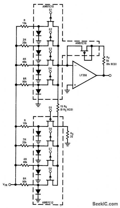
8-bit multiplying D/A converter using cascaded 4-bit sections provides logic-controlled gain for signal preconditioning, level control, and dynamic range expansion. Logic 0 turns JFET switch on, and logic 1 turns switch off. Series FET in feed-back path of opamp compensates for ON resistance of JFET switch. Circuit has gain of 0.9996 (binary) with 5K feedback resistor and gain of 0.99 (BDC) with 8K feedback resistor.- FET Databook, National Semiconductor, Santa Clara, CA, 1977, p 6-47-6-49. (View)
View full Circuit Diagram | Comments | Reading(1257)
TEMPERATURE_CONTROLLED_FAN
Published:2009/7/14 3:58:00 Author:May
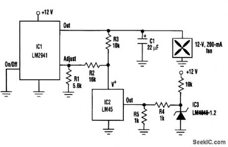
The circuit described here needs only three ICs to smoothly increase fan speed as temperature rises above an easily set trip point. Low-dropout voltage regulator ICl provides power to the fan and to temperature sensor IC2. IC2 drives the middle of the resistor divider across voltage reference IC3.Because the LM45's output stage can only source current, its output voltage will remain at about 610 mV until IC2's temperature rises above 61°C, IC2 will drive the 500-0 Thevenin resistance of the divider, which will cause IC2's supply current to increase rapidly with rising temperature. As the temperature rises above the point where IC2's output voltage exceeds the Thevenin voltage set by R4 and R5, IC2's supply current increases. IC2's supply current flows through Rl and directly affects the regulator's output voltage. If the temperature rises 20°C above the nominal61°C threshold, the regulator's output voltage will rise to 12 V and the fan will operate at full speed. (View)
View full Circuit Diagram | Comments | Reading(178)
FOUR_STATE_AMPLIFIER
Published:2009/7/14 3:54:00 Author:May
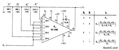
HA-2400 four-channel programmable amplifier is used with tapped voltage divider in feedback loop to give gains of 1, 2, 4, and 8 controlled by logic inputs to D0 and D1 as shown in truth table. Amplifier is noninverting.-W. G. Jung, IC Op-Amp Cookbook, Howard W. Sams, Indianapolis, IN, 1974, p 431-432. (View)
View full Circuit Diagram | Comments | Reading(795)
PHONO_PREAMP
Published:2009/7/14 3:51:00 Author:May
High input impedance of mos fet will not load ceramic cartridge rep resented by 470K and 470 pf. Q2 as emitter-follower driver transforms low input impedance of Q3 to sufficiently high value forrequired voltage gain at power output of 1 w.-V, Harrap et al.,Researchers Turn to Germanium For a MOS Field. Effect Transistor, Electronics, 37:30, p 64-68. (View)
View full Circuit Diagram | Comments | Reading(1271)
UJT_BISTABLE_RING_COUNTER
Published:2009/7/14 3:51:00 Author:May
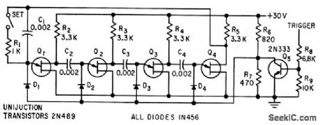
Operates up to 40,000 cps, with trigger pulse widths between 6 and 9 microsec. -T. P. Sylvan, Bistable Circuits Using Unijunction Transistors. Electronics., 31:51, p 89-91. (View)
View full Circuit Diagram | Comments | Reading(830)
10_MHz_DUAL_CHANNEL_LOGAMP
Published:2009/7/14 3:55:00 Author:May
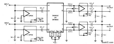
Circuitusing Texas Instruments SN56502 or SN76502 in combination,with four SN52741 oρamps、will handle 50-dB input range perchannel at all frequecies uρ to10 MHz suitable for data compression, analog computation, radar and infrared detection systems, and weapons systems. Differential output voltage levels are generally less than 0.6 V. Output swing and slope of output response are adjusted by varying gain in each channel. Coordinate origin is adjusted with offset pots of output buffers.- The Linear and Interface Circu its Data Book for Design Engineers, Texas Instruments, Dallas, TX, 1973, p 7-46. (View)
View full Circuit Diagram | Comments | Reading(1028)
PROGRAMMABLE_GAIN__OPAMP
Published:2009/7/14 3:43:00 Author:May

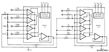
Cascading two HA-2400 digitally programmed amplifiers, each combining functions of analog switches and high-performance opamps on single IC chip, gives 16 different programmable gains in unit steps. Article gives truth table showing total gain obtained for 16 combinations of 0 and 1 on control lines D10, D11, D20, and D21. Enable lines are normally at 1, and E2 is made0 only when total gain must be zero. Applications include digital AGC and digital control of servo-systems and level detectors.-J. A. Connelly, N.C. Currie, and D. S. Bonnet, Op Amp Has 16-Step Digital Gain Control, EDN Magazine, May 5, 1974, p 75 and 77. (View)
View full Circuit Diagram | Comments | Reading(907)
| Pages:71/250 At 206162636465666768697071727374757677787980Under 20 |
Circuit Categories
power supply circuit
Amplifier Circuit
Basic Circuit
LED and Light Circuit
Sensor Circuit
Signal Processing
Electrical Equipment Circuit
Control Circuit
Remote Control Circuit
A/D-D/A Converter Circuit
Audio Circuit
Measuring and Test Circuit
Communication Circuit
Computer-Related Circuit
555 Circuit
Automotive Circuit
Repairing Circuit