
Amplifier Circuit
Index 81
MINIATURE_AUDIO_POWER_AMPLIFIER
Published:2009/7/12 23:38:00 Author:May
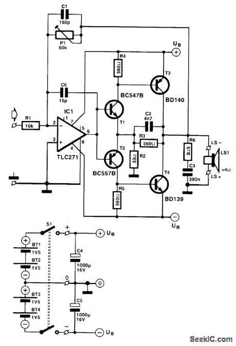
A compact audio poirer amplifier with low current drain has many applications. These are the design basis for the mini amplifier. It continues working satisfactorily with a battery voltage down to 1.5 V. Its quiescent current drain is about 1 mA, and its efficiency is a worthwhile 70 percent. It provides an output power of 500 mW into 8 Ω (or 800 mW into 4 Ω), has a sensitivity of 400 mV, and its distortion is never higher than 1.2 percent. Because the output transistors have no emitter resistor, the voltage is determined solely by the knee voltage of T3 and T4. With a load of 4 to 8 Ω, these voltages are limited to 0.2 to 0.3 V so that the transistors can be driven virtually up to the supply voltage. The overall bandwidth of the amplifier is limited to not less than 21 kHz at the maximum amplification of x5. With a 4-Ωload, the peak output current is 700 mA. A 315-mA fuse in series with the output is, therefore, a simple but effective short-circuit protection. At maximum drive with a music signal, the average current is only 50 mA. In operation the drive will never be continuously maximum, so the actual current drain will be much lower. A set of four penlight batteries should last about 200 hours.
(View)
View full Circuit Diagram | Comments | Reading(2084)
STEREO_PREAMP
Published:2009/7/12 23:35:00 Author:May
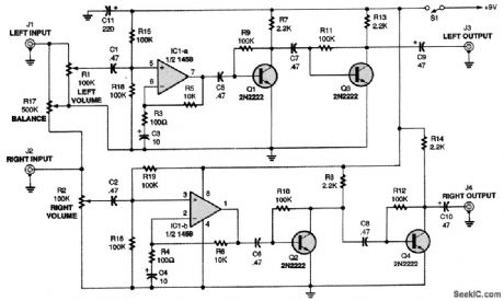
The output of the audio source is fed to the left and right inputs of the circuit (J1 and J2). Potentiometers R1 and R2 control the volumes of the input signals, while potentiometer R17 is a balance control. The incoming signals are coupled through capacitors C1 and C2 to the noninverting inputs of op amps IC1-a and IC1-b. Because IC1 operates as a single-supply amplifier, its output signal fluctuates above and below half of the supply voltage. The output signals of the op amps are coupled to the bases of two 2N2222 transistors (Q1 and Q2), which further amplify the left and right signals. Then, the outputs of the transistors are coupled to the bases of two more 2N2222 transistors (Q3 and Q4), further boosting the left and right signals. The transistor pairs also act as buffers.
(View)
View full Circuit Diagram | Comments | Reading(1751)
Z_AXIS_AMPLIFIER
Published:2009/7/16 21:24:00 Author:Jessie
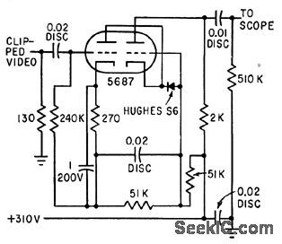
Accepts dipped video signal of microwave interferometer system and intensity-modulates electron beam of oscilloscope.-H. L. Bunn, Determining Electron Density and Distribution in Plasmas, Electronics, 34:14, p 71-75. (View)
View full Circuit Diagram | Comments | Reading(812)
STABLE_LM386_AUDIO_AMPLIFIER_CIRCUIT
Published:2009/7/12 23:34:00 Author:May
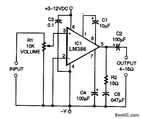
The circuit shown has components installed to improve the stability of the LM386 circuit. R2, C3, C4, and C5 are sometimes omitted, leading to instability with certain layouts. These components should be used to ensure stability. Output is up to 1 W, depending on supply voltage and load impedance. (View)
View full Circuit Diagram | Comments | Reading(2466)
60_W_SWITCHING_AMPLIFIER
Published:2009/7/12 23:32:00 Author:May
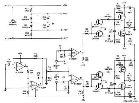
The schematic for the switching amplifier is shown. A separate 51-Vdc source is required to power the amplifier circuit. The 51-Vdc source is fed to a pair of zener diodes, D5 and D6, and is fi1tered by capacitors C11 and C12 to provide a 12-Vdc source for part of the circuit. Also, part of the 51-Vdc source bypasses the zeners to power the sections of the circuit that require a high voltage. The right and left signals are input to the amplifier through jacks J1 and J2, respectively. Two sections of a TL074 op amp, IC1-c and IC1-d, generate a 4-V p-p, 50-kHz triangular reference waveform. The generated waveform is then fed to potentiometer R19. That enables the amplifier to use input signals with amplitudes ranging from 1 V p-p to 4 V p-p. The other two op-amp sections, IC1-a and IC1-b, function as comparators to produce the pulse -width-modulating output for the left and right channels of the amplifier. In the right channel of the amplifier, the output of the voltage comparator is coupled to the bipolar translating circuit through a current-limiting resistor, R5. The translating circuit has a positive and a negative leg; Q1, D1, and R7 make up the positive leg, and Q3, D3, and R11 make up the negative leg. Both legs are tied to ground through the emitters of Q1 and Q3, providing a reference point for the translator. The translator arrangement results in 17 V being present across Q1, Q3, and zener diodes D1 and D3. Sufficient current is then present to overcome the power MOSFET gate capacitance; that rapidly switches on and off the power MOSFET complementary push-pull output stage, composed of Q5 and Q7. Resistor R3 keeps the output swing centered at the midpoint of the supply voltage. Without R3, the square-wave output drifts down toward the negative rail. The RC network, composed of R9 and C5, which connects to both N- and P-channel gates, minimizes switching noise and sharpens the square-wave output. Note that both channels contain power-supply elements to split the incoming single-polarity voltage in half. Capacitors C3, C4, C7, and C8 make up a series-parallel circuit that converts the 51-Vdc supply to 25.5 Vdc. The output can feed full-range 60-W rms speakers, which demodulate the signal and produce an amplified audio output. (At peak output power, the current draw for an 8- Ω dynamic load is approximately 1.2 A at 51 Vdc.) (View)
View full Circuit Diagram | Comments | Reading(5012)
GYRO_VIBRATION_AMPLIFIER
Published:2009/7/16 21:15:00 Author:Jessie
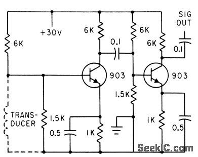
Vibration resulting from imbalance is sensed by inductive transducer that produces sine wave which is amplified by circuit and displayed on cro.-F.W. Kear,Electronic System for Balancing Gyro Wheels, Electronics, 33:43, p 82-85. (View)
View full Circuit Diagram | Comments | Reading(873)
PORTABLE_CRO_HORIZONTAL_AMPLIFIER
Published:2009/7/16 21:12:00 Author:Jessie
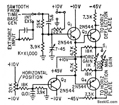
Balanced circuit includes temperature compensation. Closing S1 provides magnification of 5 on screen. Bandwidth is 1 Mc.-O. Svehaug and J. R. Kobbe, Battery-Operated Transistor Oscilloscope, Electronics, 33:12, p 80-83. (View)
View full Circuit Diagram | Comments | Reading(886)
10_GHz_WAVEMETER_AMPLIFIER
Published:2009/7/12 23:12:00 Author:May
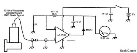
This wavemeter amplifier is connected to the microwave waveguide detector. This circuit operates from a single 9-V transistor radio battery for simplicity.
(View)
View full Circuit Diagram | Comments | Reading(1711)
PORTABLE_CRO_UNBLANKING_AMPLIFIER
Published:2009/7/16 20:58:00 Author:Jessie
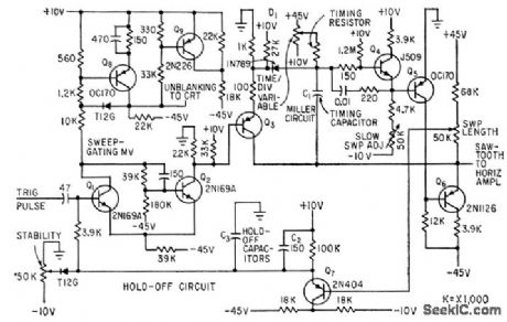
Supplies signal to turn on crt during sweep,Hold-off circuit insures that trace starts from same point on every sweep.-O. Svehaug and J.R. Kobbe,Battery-Operated Transistor Oscilloscope, Electronics, 33:12, p 80-83. (View)
View full Circuit Diagram | Comments | Reading(809)
D_C_TO_100_MC_DEFLECTION_AMPLIFIER
Published:2009/7/16 20:53:00 Author:Jessie
Gain is constant within 3 db of 40 db over entire 100-Mc bandwidth, for driving electrostatic deflection plates of oscilloscope.-L.L.Kossakowski,Designing a D-C to 100-MC Deflection Amplifier, Electronics, 35:17, p 64-66. (View)
View full Circuit Diagram | Comments | Reading(846)
MOBILE_±_35_V_5_A_AUDIO_AMPLIFIER_SUPPLY
Published:2009/7/16 20:53:00 Author:Jessie
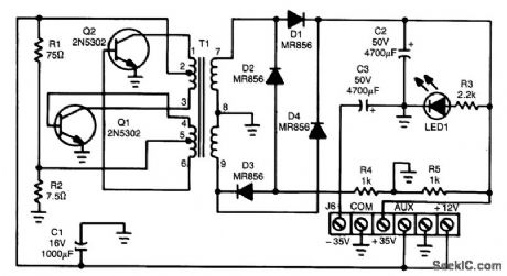

This ± 35-V supply uses a two-transistor multivibrator with a toroidal transformer. The transformer core is obtainable from Magnetics, Inc. Specifications for T1 are:
(View)
View full Circuit Diagram | Comments | Reading(1079)
PORTABLE_CRO_TRIGGER_INPUI_AMPLIFIER
Published:2009/7/16 20:52:00 Author:Jessie
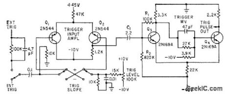
Schmitt trigger mvbr Q3-Q4 is modified by R1, R2, and C1 to give stable presentation at 2 Mc, with synchronization up to 4 Mc.-O. Svehaug and J. R.Kobbe,Battery Operated Transistor Oscilloscope, Electronics, 33:12, p 80-83. (View)
View full Circuit Diagram | Comments | Reading(821)
BOOTSTRAPPED_AMP_CURRENT_SOURCE
Published:2009/7/16 20:51:00 Author:Jessie
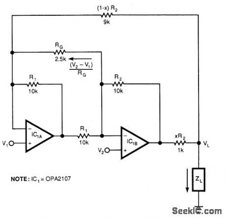
This circuit responds to the difference between V1 and V2. RG on sets gain. Resistors XR2 and (1 -X) R2 produce the bootstrap effect. These two resistors convert the circuit's output voltage to a current. IC1 and IC2 are Burr-Brown OPA2107 or equal. (View)
View full Circuit Diagram | Comments | Reading(857)
Ear Drop Amplification Circuit
Published:2011/7/17 23:32:00 Author:Felicity | Keyword: Ear Drop, Amplification Circuit
View full Circuit Diagram | Comments | Reading(721)
SINGLE_POT_SWINGS_AMPLIFIER_GAIN_POSITIVE_OR_NEGATIVE
Published:2009/7/16 22:12:00 Author:Jessie
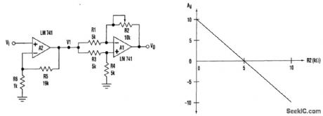
It is handy to have a gain block with a gain that can be varied smoothly from positive to negative with a single potentiometer. The circuit shown accomplishes this function with R2. Op amp A1 is configured with both inputs tied together. Op amp A2 functions as a buffer. WithR1=R3=R4=R=5KΩ,the gain of the differential amplifier is given by AV1=(V0/V1)=1/2(1-R2/R). With a buffer amplifier gain of 20, the overall gain of the amplifier is given by AV=(V0/V1)=10(1-R2/R). By using a 10-turn potentiometer, the gain can be varied from positive to negative. (View)
View full Circuit Diagram | Comments | Reading(839)
CHARACTER_DEFLECTION_AMPLIFIER
Published:2009/7/16 21:52:00 Author:Jessie
Converts X or Y voltage waveform into equivalent current waveform of up to 0.5 amp peak to peak, to drive low-inductance defection yoke of cathode-ray character generator.-K. E. Perry and E. J. Aho, Radar. Computer Display Traces Alphanumeric Characters, Electronics, 34:26, p 75-79. (View)
View full Circuit Diagram | Comments | Reading(844)
DYNAMIC_MICROPHONE_PREAMP
Published:2009/7/16 21:42:00 Author:Jessie
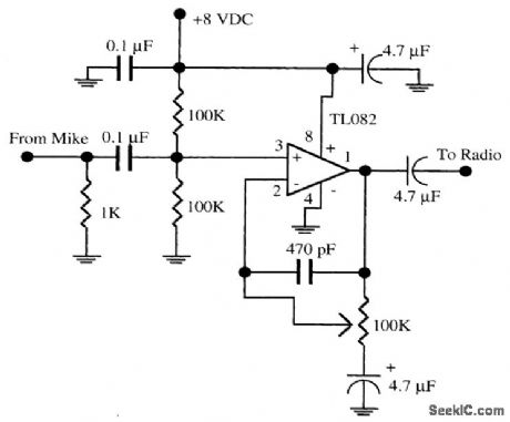
This circuit uses a TL082 op amp to boost the output of a dynamic mike to a level sufficient for a radio transceiver, audio amplifier, or PA system. (View)
View full Circuit Diagram | Comments | Reading(9055)
McIntosh C22 Phono Pre-amp Circuit
Published:2011/7/18 3:08:00 Author:Felicity | Keyword: McIntosh C22 Phono Pre-amp Circuit
View full Circuit Diagram | Comments | Reading(5988)
TUNNEL_DIODE_PULSEHEIGHT_DISCRIMINA_TOR
Published:2009/7/16 22:47:00 Author:Jessie
Used to analyze 30,nsec pulses varying in height from 0 to 6 v peak, over temperature range of -20 to +60°C, Ten stages were connected in parallel and 0.5.v steps used for 0 to 5 v output range. When tunnel diode is triggered at its predetermined level, Q1 delivers fixed current to operational amplifier. As input pulse height increases, more and more tunnel diodes are triggered, and current to operational amplifier increases linearly.-J. D. Nickell, tunnel-Diode Pulse-Height Discriminator, EEE, 13:9, p 75. (View)
View full Circuit Diagram | Comments | Reading(967)
SIGNAL_AMPLITUDE_ANALYZER
Published:2009/7/16 22:43:00 Author:Jessie
Width of rectangular output pulse is proportional to time spent by signal between specified voltage levels. Used to determine probability amplitude density functions,-T. A. Bickart, Amplitude Slicer for Signal Analysis Electronics 32:9, p 64-65. (View)
View full Circuit Diagram | Comments | Reading(789)
| Pages:81/250 At 2081828384858687888990919293949596979899100Under 20 |
Circuit Categories
power supply circuit
Amplifier Circuit
Basic Circuit
LED and Light Circuit
Sensor Circuit
Signal Processing
Electrical Equipment Circuit
Control Circuit
Remote Control Circuit
A/D-D/A Converter Circuit
Audio Circuit
Measuring and Test Circuit
Communication Circuit
Computer-Related Circuit
555 Circuit
Automotive Circuit
Repairing Circuit