
Amplifier Circuit
Index 93
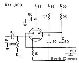
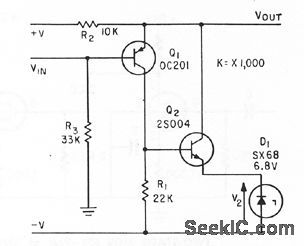
Op_amp_with_FET_AGC_circuit_
Published:2009/7/19 21:10:00 Author:Jessie
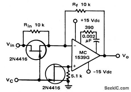
Op amp with FET AGC circuit (courtesy Motorola Semiconductor Products Inc.). (View)
View full Circuit Diagram | Comments | Reading(2271)
Simple_differentiator_using_an_ECG941_941D_941M_operational_amplifier
Published:2009/7/19 21:09:00 Author:Jessie
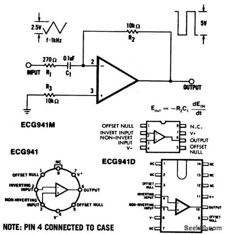
Simple differentiator using an ECG941/941D/941M operational amplifier. Typical supply voltage is ±15volts (courtesy GTE Sylvania Incorporated). (View)
View full Circuit Diagram | Comments | Reading(721)
Feedforward_frequency_compensation_circuit_using_an_AD101A_201A_301A_op_amp
Published:2009/7/19 21:09:00 Author:Jessie
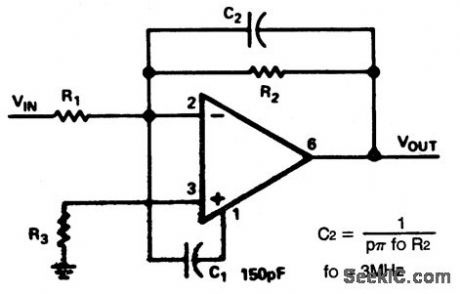
Feedforward frequency compensation circuit using an AD101A/201A/301A op amp. Typical supply voltage is ±15 volts (courtesy Analog Devices, Inc.). (View)
View full Circuit Diagram | Comments | Reading(966)
Inverting_amplifier_using_an_ECG941_941D_941M_operational_amplifier
Published:2009/7/19 21:08:00 Author:Jessie
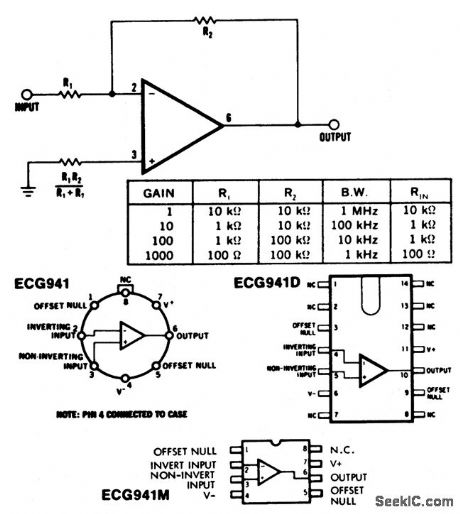
Inverting amplifier using an ECG941/941D/941M operational amplifier. Typical supply voltage is ±15 volts (courtesy GTE Sylvania Incorporated). (View)
View full Circuit Diagram | Comments | Reading(723)
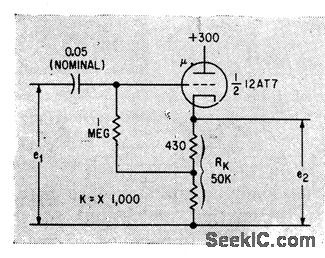
Differential_amplifier_using_an_MC1539_op_amp
Published:2009/7/19 21:07:00 Author:Jessie
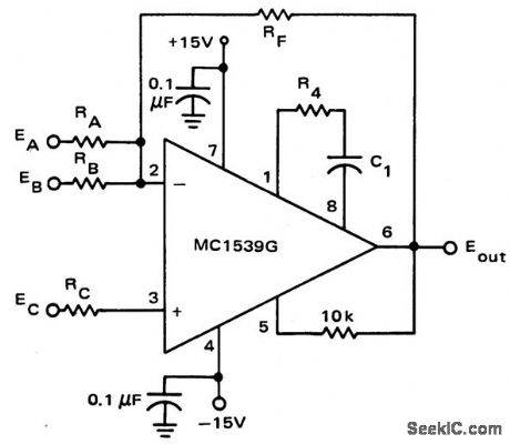
Differential amplifier using an MC1539 op amp (courtesy Motorola Semiconductor Products Inc.). (View)
View full Circuit Diagram | Comments | Reading(842)
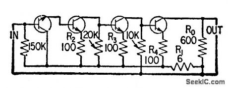
GAIN_CONTROLLED_AMPLIFIER
Published:2009/7/10 3:36:00 Author:May
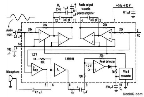
This single-chip circuit adjusts its audio gain according to the ambient nolse picked up by the mlcrophone。When operating in a quiet environment,the audio output is quiet,while a notsy environment resultsh a louder audio output。Audio to pm 13 is amplified by the variable-gain amplifier within the LM1894 IC,Audio from the microphone connected through 0.1μF capacitor to pin 6 controls the audio gain of thevariable-gam amplifier,The output appears on pm 11 andis taken off through an 0.1μ capacitor. (View)
View full Circuit Diagram | Comments | Reading(0)
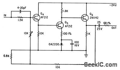
ANALOG_PREAMP
Published:2009/7/10 3:28:00 Author:May
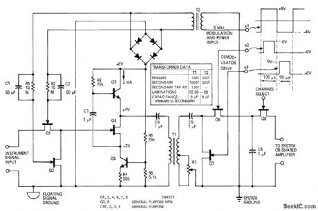
Combination of 5-kHz FET-chopper amplifier Q1-Q2 with transformer isolation of signal and system grounds gives low-cost analog instrumentation amplifier that will process millivolt DC signals while rejecting hundreds of volts of common-mode DC. Signal accuracy is 0.1% for inputs between 50 and 500mV. Input impedance is 4 megohms, drift is only 0.2μV/℃, and DC common-mode rejection rate is better than 120 dB. Low-impedance output of followers Q3-Q4-Q5 is sent through T1 to synchronousFET demodulator Q6-Q7,R7 adjusts system scaling.C.A.Walton,High-CMR,Low-Cost DC Instrumentation Preamp,EDN Magazine,Jan 15,1971,p 47-48. (View)
View full Circuit Diagram | Comments | Reading(924)
GATED_AMPLIFIER_FOR_RECEIVER
Published:2009/7/19 21:54:00 Author:Jessie
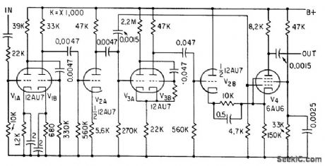
Input from f-m discriminator of ground receiver for neutron-detecting radiosonde contains two sub-carrier oscillator frequencies plus sleep un wanted pulses at audio blocking rate of 10 to 200 cps. Three-stage amplifier feeds amplified input signals to one-shot mvbr V3A-V3B for blocking of unwanted pulses. Out-put of gated amplifer V4 then contains only bursts of the two desired subcarrier frequencies.-L. Hillman and It. C. Haymes, Modifying a Telemetry System for Balloon-Borne Neutron Detection, Electronics, 34:11, p 60-63. (View)
View full Circuit Diagram | Comments | Reading(724)
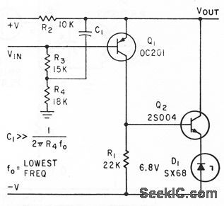
BOOSTING_INPUT_IMPEDANCE
Published:2009/7/10 2:27:00 Author:May
Circuit shows how voltage gain in transistor amplifier can be exchanged for input impedance through use of negative feedback. At same time, voltage gain is made more independent of transistor parameters. -Feedback Increases Input Impedance, Electronics, 32:11, p 150-153. (View)
View full Circuit Diagram | Comments | Reading(756)
TRIODE_CATHODE_FOLLOWER
Published:2009/7/10 2:27:00 Author:May
Effective gain stability factor is approximately equal to reciprocal of omplification factor of tube.-G.M. Davidson and R. F. Brady, Unity-Gain AmpliGer Offers High Stability, Electronics, 33:9, p 66-67. (View)
View full Circuit Diagram | Comments | Reading(967)
CABLE_DRIVING_AMPLIFIER
Published:2009/7/10 2:24:00 Author:May
Used between wideband integrator and l85-ohm cable. With voltage gain of 3, bandwidth is l8 Mc without overshoot for pulse signcds.-S.Berglund and so Westerlund,Probes for Plosma Research with Wideband Integrators,Electronics,35:24,p 44-45. (View)
View full Circuit Diagram | Comments | Reading(694)
SECONDARY_EMISSION_PENTODE_CATHODE_FOLLOWER
Published:2009/7/10 2:21:00 Author:May
Circuit is enhanced by connecting dynode bock to cathode. Uses degenerative feedback, to achieve high-performance impedance transformation. Can be used to match high-impedance source to low-impedonce load.-E. J. Martin, Jr., How to Use the Secondary-Emission Pentode, Electronics, 33:41, p 60-63. (View)
View full Circuit Diagram | Comments | Reading(740)
CATHODE_EOLLOWER_WITH_099963_GAIN
Published:2009/7/10 2:20:00 Author:May
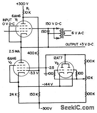
Used to couple high-impedance source to low-impedance output without attenuating or loading source signal. Output impedance is 50 ohms and respomse is lat within 3 db front d-c to 250 kc. Circuit delivers outputs from -140 to +210 v at -0.8 to +2 ma.Feedback through pentade helps maintain unity gain.-Cathode-Follower Gain Approaches Unity, Electronics, 31:1, p 94-96.
(View)
View full Circuit Diagram | Comments | Reading(700)
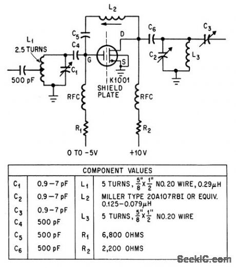
TUNED_10_MC_AMPLIFIER_WITHOUT_NEU_TRALIZATION
Published:2009/7/10 2:18:00 Author:May
Low reverse transfer of cascade connection makes possible stable operation of commonsource fet. Transducer gains are 20.6 db and 25.3 db for 2N2497 and 2N2499 respectively.-Texas Instrumens Inc., Solid-State Communications, Mc Graw-Hill, N.Y., 1966, p 142. (View)
View full Circuit Diagram | Comments | Reading(745)
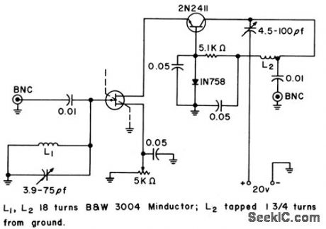
200_MC_FET_NEUTRALIZED_AMPLIFIER
Published:2009/7/10 2:11:00 Author:May
Capacitor C5 between dmin and gate provides neutralization by nullifying feedback. Neutrctlized stable gain at 250 Mc is 8 db. Bandwidth is 12 Mc.-P. E. Kolk and I. A. Maloff, The Field-Effect Transistor as High-Frequency Ampliler, Electronics, 37:31, p 71-74. (View)
View full Circuit Diagram | Comments | Reading(604)
MODIFIED_EMITTER_SQUARED_EOLLOWER
Published:2009/7/10 2:07:00 Author:May
Complementary transistor arrangement of feedback amplifier is modiled to reduce shunting effect of R3 by applying positive feedback voltage that artificially increases vctlue of R3.-T. K. Hemingway and J. Willis, Transistor Pairs Improve Emitter-Follower Performance, Electronics, 35:21, p 48-49. (View)
View full Circuit Diagram | Comments | Reading(751)
COMPOUNDED_EMITTER_FOLLOWER
Published:2009/7/10 2:01:00 Author:May
Compounded emitter-follower with feedback, operctted as complementary pair, gives higher input impedance, higher gain, and lower output impedance than conventionol eminerfollower.-T. K. Hemingway and J. Willis, Transistor Pairs Improve Emitter-Follower Performance, Electronics, 35:21, p 48-49. (View)
View full Circuit Diagram | Comments | Reading(780)
SMALL_SIGNAL_60_MC
Published:2009/7/10 1:56:00 Author:May
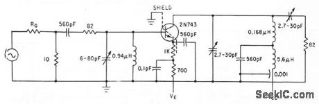
Epitaxial 2N743 is operated Gammon-emitter at signal frequency and Gammon-base for biasing. Unneufralized gain per stage is 17 db.-D. Hall, Using Epitaxial Transistors in Switching and R.F Circuits, Electronics, 34:13, p 52-53. (View)
View full Circuit Diagram | Comments | Reading(637)
CASCODE_FOLLOWER
Published:2009/7/10 1:54:00 Author:May
Output is 20 v peak-to-peak into 1,000 ohms, down to 5 cps, with high stability.-R. W. Johnson, Circuit with a Twist: The cascode 36:49,p 69-70. (View)
View full Circuit Diagram | Comments | Reading(824)
FET_SOURCE_FOLLOWER
Published:2009/7/10 1:53:00 Author:May
Voltage-divider biasing increases input impedance. R3 provides negative feedback.-B. Down, Using Feedback in FET Circuit to Reduce Input Capacitance, Electronics, 37:31, p 63-65.
(View)
View full Circuit Diagram | Comments | Reading(1246)
| Pages:93/250 At 2081828384858687888990919293949596979899100Under 20 |
Circuit Categories
power supply circuit
Amplifier Circuit
Basic Circuit
LED and Light Circuit
Sensor Circuit
Signal Processing
Electrical Equipment Circuit
Control Circuit
Remote Control Circuit
A/D-D/A Converter Circuit
Audio Circuit
Measuring and Test Circuit
Communication Circuit
Computer-Related Circuit
555 Circuit
Automotive Circuit
Repairing Circuit