
Amplifier Circuit
Index 94
4_watt_AF_amplifier_using_an_ECG735_class_A_driver_and_an_ECG153_audio_output
Published:2009/7/20 1:43:00 Author:Jessie
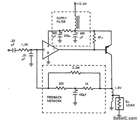

4-watt AF amplifier using an ECG735 class A driver and an ECG153 audio output. This is a typical automotive tape player amplifier (courtesy GTE Sylvania Incorporated).
(View)
View full Circuit Diagram | Comments | Reading(603)
LOW_NOISE_FET_AMPLIFIER
Published:2009/7/10 1:52:00 Author:May
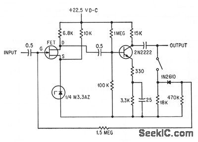
Agc feedbackextends imput level to 150 mv.-L.E.Clark,E.B.Mack,and R.C.Heihall,Highlights of Small-Signal Circuit Design,Electronics,36;49,p 46-50. (View)
View full Circuit Diagram | Comments | Reading(818)
Stereo_phono_AF_preamplifier_with_RIAA_equalization
Published:2009/7/20 1:41:00 Author:Jessie
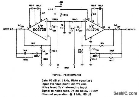
Stereo phono AF preamplifier with RIAA equalization. Gain is 40 dB at 1 kHz with the input overload point set at 80 mV RMS. Noise level is 2 μV referred to the input. Signal to noise ratio is 74 dB below 10 mV. Channel separation at 1 kHz is 80 dB (courtesy GTE Sylvania Incorporated). (View)
View full Circuit Diagram | Comments | Reading(859)
GROUNDED_GRID_BROADBAND
Published:2009/7/10 1:48:00 Author:May

Grounded-cathode preamplifier has plate load that provides increasing gain with increasing frequency to drive following two tubes in cascade. Both source and load impedances are 50 ohms.-Broadband VHF Amplifier Covers 30 to 260 Mc Range, Electronics, 35:4, p 102. (View)
View full Circuit Diagram | Comments | Reading(839)
DUTY_CYCLE_MEASURER
Published:2009/7/10 1:48:00 Author:May
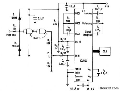
An Intersil 7101 31/2-digit A/D converter is used to display the duty cycle of a pulse train as a percent-age. The frequency range of this circuit is 100 Hz to 250 kHz. The CM0S gates convert the pulse train to constant amplitude. This amplitude is then compared to a reference of 1V, derived from R3 and R4. P1 is for calibration. (View)
View full Circuit Diagram | Comments | Reading(636)
Stereo_tape_system_AF_preamplifier_with_simple_tone_control
Published:2009/7/20 1:38:00 Author:Jessie
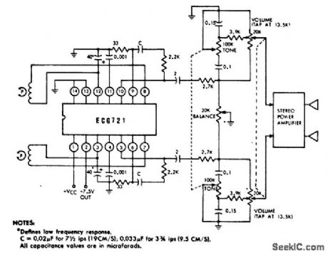
Stereo tape system AF preamplifier with simple tone control. Current drain at 12 volts is typically 16 mA. Voltage gain is 68 dB. Channel separation is typically 60 dB (courtesy GTE Sylvania Incorporated). (View)
View full Circuit Diagram | Comments | Reading(891)
Stereo_record_player_AF_preamplifier_with_bass_and_treble_controls_for_magnetic_pickup
Published:2009/7/20 1:37:00 Author:Jessie
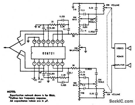
Stereo record player AF preamplifier, with bass and treble controls, for magnetic pickup. Current drain is typically 16 mA at 12 volts. Voltage gain is 68 dB. Channel separation is typically 60 dB (courtesy GTE Sylvania Incorporated). (View)
View full Circuit Diagram | Comments | Reading(1052)
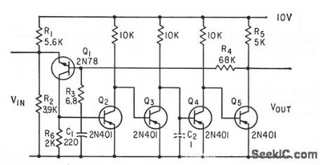
STABILIZED_DIRECT_COUPLED_A_C_AMPLIFIER
Published:2009/7/10 1:47:00 Author:May
Current-derived stabilization gives simple ampliler using only one capacitor. Adding C2 improves stability but lowers cutoff frequency.-P. Laakmann, Direct Coupling Shrinks Amplifer Size and Cost, Electronics, 36:12, p 66-48. (View)
View full Circuit Diagram | Comments | Reading(810)
UNITY_GAIN_BUFFER
Published:2009/7/10 1:47:00 Author:May
Positive gain of unity is obtained with high input impedance, low output impedance, negligible phase shift, and without phase reversal. Can be used for isolating resolvers from loads.-D. K. Phillips, Unity-Gain Buffer Acquires Precision by Feed-back, Electronics, 36:51, p 36-37. (View)
View full Circuit Diagram | Comments | Reading(0)
NEUTRALIZED_MOS_FET
Published:2009/7/10 1:45:00 Author:May
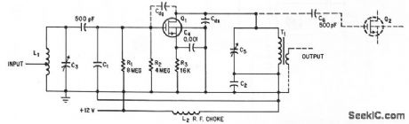
Delivers power gain of 20 db at 100 Mc, with common-source connection.-G.C.Luettgenau and S.H.Barnes,Designing With Low-Noise MOS FETs:A Little Different But No Harder,Electronics,37:31,p 53-58. (View)
View full Circuit Diagram | Comments | Reading(675)
SOURCE_FOLLOWER_USES_BOOTSTRAPPING
Published:2009/7/10 1:44:00 Author:May
Bandwidth is 10 cps to 10 kc, d-c input impedance is 10 meg, and input impedance at 10 kc is above 1 meg for input signals from 1 my to 10 my.-T. R. Bignell, How to Get Maximum Input Impedance with Field-Effect Transistors, Electronics, 36;10, p 44-46. (View)
View full Circuit Diagram | Comments | Reading(770)
BROADBAND_WITH_GAIN_OF_1350
Published:2009/7/10 1:43:00 Author:May
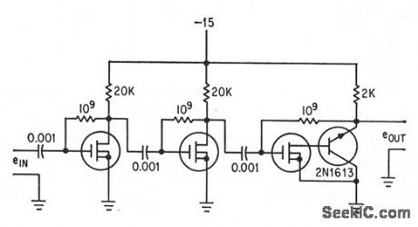
Metal oxide semkonductor transistors (p-mosts) in Darlington contguration give high input impedance and low output impedance from 5 cps to 72 kc.-F. M. Wanklss, Novel Field-Effect Devke Provides Broadband Gain, Electronics, 36A4, p 30-33. (View)
View full Circuit Diagram | Comments | Reading(809)
1_watt_power_amplifier
Published:2009/7/20 1:36:00 Author:Jessie
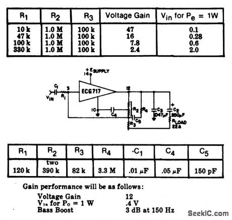
1-watt power amplifier. Refer to the table to select the desired voltage gain. In the circuit the AC feedback path is different from the DC path. Resistor R2 is bypassed to ground, taking it out of the AC feedback loop. The voltage gain is determined by the ratio of R4/R1. Another feature of this circuit is that you can introduce bass boost by the selection of capacitor values for C1, C4 and C5. With the values shown in the table at the bottom of the figure, gain performance is as follows: voltage gain is 12, VIN for Po at 1W is 0.4 volt, and bass boost is 3 dB at 150 Hz (courtesy GTE Sylvania Incorporated). (View)
View full Circuit Diagram | Comments | Reading(796)
General_purpose_fixed_gain_low_distortion_amplifier_using_an_ECG716_that_can_be_employed_for_such_things_as_a_telephone_or_headset_AF_amplifier
Published:2009/7/20 1:34:00 Author:Jessie
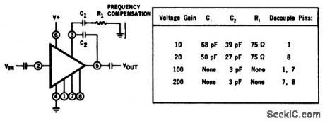
General-purpose fixed-gain low-distortion amplifier, using an ECG716, that can be employed for such things as a telephone or headset AF amplifier. Fixed voltage gain of 10, 20, 100, and 200 can be obtained by referring to the table. Supply voltage is 27 volts, input voltage is ±5 volts, and power dissipation is 600 mW. Voltage gain falls off sharply above 1 MHz (courtesy GTE Sylvania Incorporated). (View)
View full Circuit Diagram | Comments | Reading(647)
SOURCE_FOLLOWER_WITH_REDUCED_GATE_TO_DRAIN_CAPACITANCE
Published:2009/7/10 1:42:00 Author:May
Diode D1 gives maximum a-c bootstrapping of gate bias resistance while providing required d.c bias. Emitter-follower Q2 couples to drain of let al a signal in phase with input, to give extremely low input capacitance.-T. R. Bignall, How to Get Maximum Input Impedance with Field-Effect Transistors, Electronics, 36:10, p 44-46. (View)
View full Circuit Diagram | Comments | Reading(804)
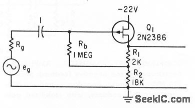
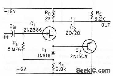
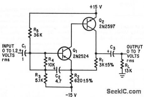
CURRENT_DERIVED__STABILIZATION
Published:2009/7/10 1:41:00 Author:May
Bridge-derived stabilization In direct-coupled a-c amplifier Provdes current sensitivity of 0.1 microamp per ma of output current.-P.Laakmann, Direct Coupling Shrinks Ampliler Size and Cost, Electronics, 36:12, p 66-68. (View)
View full Circuit Diagram | Comments | Reading(662)
250_MC_12_W_POWER_AMPLIFIER
Published:2009/7/10 1:39:00 Author:May
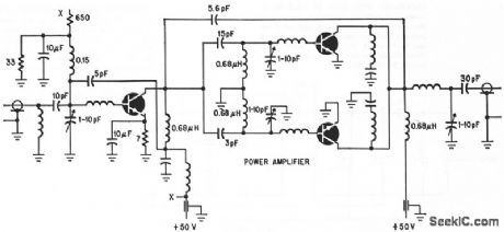
Commonemitter circuits operating class C serve for driver and parallel-connected power amplifier transistors.Total gain is 12 db.-N.Downs and B.van Sutphin, Solid-State Transmitter Ready for UHF Telemetry,Electronics,37:17,p 76-80. (View)
View full Circuit Diagram | Comments | Reading(744)
COMPLEMENTARY_IRANSISIOR_AMPLIFIER
Published:2009/7/10 1:38:00 Author:May
Bootstrapping and negctive loodback Provide 220,000-ohm input impedance and 60,000-ohm ootput impedance with stabilized gain over wide temperaturer range.-L.J.Ernst,Complementary Electronics,37:16,p 92-93. (View)
View full Circuit Diagram | Comments | Reading(707)
DISCRIMINATOR__AMPLIFIER
Published:2009/7/10 1:36:00 Author:May
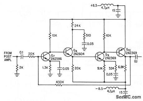
Direct-coupled voltage amplifier of with a-c couplifig at input and output has loop gain of 36 for bond-width of 1 Mc, including low-impedance driver biting Q10.-R. Cuikay and T.Callahan,Or-biting Observatory to Measure Stars'Dim Light,Electronics,37:9,p 28-31. (View)
View full Circuit Diagram | Comments | Reading(710)
100_MC_FET_AMPLIFIER
Published:2009/7/10 1:33:00 Author:May
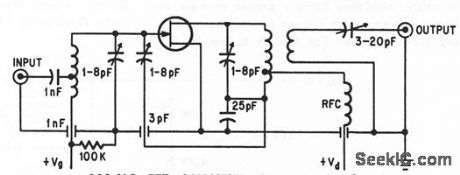
Low-cost insulaled-gate fet circuit can handle signals up to signal volts in uhf range, with inherently low cross.modulation distortion. -Low.Cost Power Booster, Electronics, 37:14, p 29-30. (View)
View full Circuit Diagram | Comments | Reading(722)
| Pages:94/250 At 2081828384858687888990919293949596979899100Under 20 |
Circuit Categories
power supply circuit
Amplifier Circuit
Basic Circuit
LED and Light Circuit
Sensor Circuit
Signal Processing
Electrical Equipment Circuit
Control Circuit
Remote Control Circuit
A/D-D/A Converter Circuit
Audio Circuit
Measuring and Test Circuit
Communication Circuit
Computer-Related Circuit
555 Circuit
Automotive Circuit
Repairing Circuit