
Amplifier Circuit
Index 99
65_watt_AF_power_amplifier_using_an_ECG1078_chip_powered_by_±12_volt_supplies
Published:2009/7/20 4:28:00 Author:Jessie

6.5-watt AF power amplifier using an ECG1078 chip powered by ±12-volt supplies. Frequency response is from 100 hertz to 20 kilohertz (courtesy GTE Sylvania Incorporated). (View)
View full Circuit Diagram | Comments | Reading(961)
Equalizer_amplifier_for_cassette_tape_recorders_using_an_ECG1087_module
Published:2009/7/20 4:27:00 Author:Jessie
Equalizer amplifier for cassette tape recorders using an ECG1087 module. Typical voltage gain is 35 dB (courtesy GTE Sylvania Incorporated). (View)
View full Circuit Diagram | Comments | Reading(605)
400_Hz_AMPLIFIER_WITH_95_dB_CMRR
Published:2009/7/9 21:36:00 Author:May
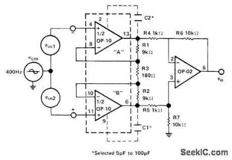
Precision Monolithics OP-10 dual opamp driving 0P-02 opamp gives high common-mode rejection ratio. CMRR is optimized by selecting C1 and C2 in range of 5 to 100 pF for minimum output e0 as viewed on CRO whilefeeding±10 V signal at 400 Hz to common connection of inputs.-''Linear &Conversion I.C.Products,''Precision Monolithics,Santa Clara,CA,1977-1978,p 15-2.
(View)
View full Circuit Diagram | Comments | Reading(678)
BURGLAR_ALARM_WITH_TIMED_SHUTOFF
Published:2009/7/9 21:36:00 Author:May
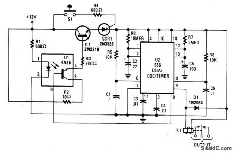
When S1 (sensor) is closed, power is applied to U2, a dual timer, After a time determined by C2, C1 is energized after a predetermined time determined by the value of C5, pin 9 of U2 becomes low, switching off the transistor in the optoisolater, cutting anode current of SCR1 and de-energizing K1. The system is now reset. Notice that (R6× C2) is less than (R7× C5). The ON time is approximately given by:
(R7×C5)-(R6×C2))=tON (View)
View full Circuit Diagram | Comments | Reading(1590)
OSCILLOSCOPE_PREAMP
Published:2009/7/9 21:30:00 Author:May
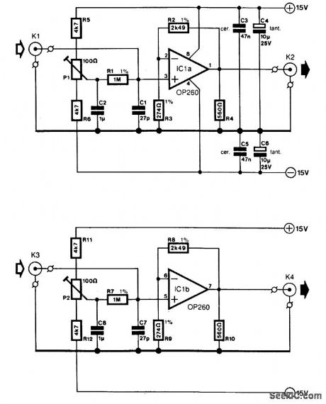
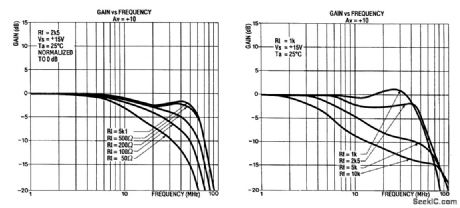
In many oscilloscopes, The most sensitive range is 2 to 5 mV, although it is often possible to improve this to 1 to 2 mV by a variable gain control. To obtain even better sensitivity, the present prearnplifter, which has an amplification of about 10 (20 dB), might be useful.
Because most oscilloscopes have a bandwidth of 20 MHz or more, the amplifier must, of course, have a slightly wider bandwidth and that is achieved with a Type OP260 op amp. This has a slew rate of 550 V/μs (at an amplification of 10) and a bandwidth of 40 MHz that is virtually independent of the amplification.
The gain vs. frequency response is not so good, however: as can be seen from Fig. 39-1(b), where the characteristics are given for a number of loads. The hump in the curves depends on the value of the feed-back resistor, whose optimum value appears to be 2.5 kΩ.
The curves in Fig. 39-1(c) accord with different values of R2/R8 for an amplification factor of 10. Some experimentation with the value of R2/R8 for different amplification factors can be instructive. Remember, however, that the output impedance increases from 20 to 225Ω over the frequency range of 10 MHz to 60-70 MHz. It is therefore important to keep all connections on the prototyping board as short as possible and to connect all earth points to a common ground via a separate, heavy track. Also, do not use an IC socket.
An input impedance of 1 MΩ was chosen, which results in a fairly high level of noise at the output (with open-circuit input). This value can be reduced, because otherwise the use of a 1:10 probe will be inhibited; it would give constant problems with the noise. However, when the amplifier is connected to a suitable source, the noise reduction is normally more than ample to obtain a good trace on the screen.Presets Pl and P2 provide compensation for the dc offset and input offset, caused by R1 and R7 respec-tively.
The input bias current for the noninverting input is about 10 times lower than that for the inverting input, which makes the OP260 more suitable for noninverting circuits. The inverting circuit can also give problems because of the low values of R2(R8) and R3 (R9). The input bias current is typically 0.2μA, and the input offset is about 3 mV (max. 7 mV).
In this type of circuit, it is important to use a well-regulated power supply. The power-supply suppres-sion up to 10 kHz is roughly 70 dB, and this reduces with increasing frequency. Any noise or tiny ripple on the supply lines would make the application of the circuit as a small-signal amplifier impossible.
The circuit draws a current of about 14 mA. The slew rate, as with most op amps, is asymmetric and might lead to visible distortion of the signal when the drive to the 560-Ω resistor is high at the higher fre-quencies. (View)
View full Circuit Diagram | Comments | Reading(1573)
50_watt_PMS_hi_fi_amplifier_for_an_8_ohm_load
Published:2009/7/20 4:22:00 Author:Jessie
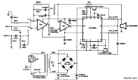
50-watt PMS hi-fi amplifier for an 8-ohm load. This circuit delivers about 56 volts peak to peak across an 8-ohm load. Distortion is about 1 % at 20 kHz. The ganged switch at the input is for selecting either disc or FM radio. The input 741 stage is a preamplifier with RIAA equalization for records (courtesy Intersil, Inc.). (View)
View full Circuit Diagram | Comments | Reading(1047)
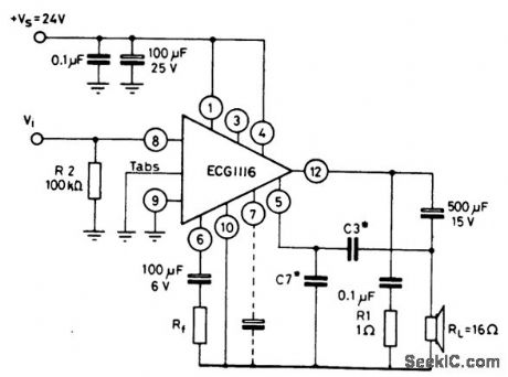
5_watt_AF_power_amplifier_with_16_ohm_load_connected_to_supply
Published:2009/7/20 4:20:00 Author:Jessie
5-watt AF power amplifier with 16-ohm load connected to supply. Capacitor C3 is typically 330 pF and C7 is 1500 pF. Generally, C7 is five times greater than C3.The ECG1116 is a 12-pin QIP. To obtain the rated output heatsinking is necessary via the two tabs. Frequency response is from 40 hertz to 20 kilohertz. Input resistance is 5M (courtesy GTE Sylvania Incorporated). (View)
View full Circuit Diagram | Comments | Reading(910)
1_watt_cassette_record_playback_amplifiers_using_an_ECG1095_14_pin_DIP
Published:2009/7/20 4:19:00 Author:Jessie
1-watt cassette record/playback amplifiers using an ECG1095 14-pin DIP. The only external transistors outside of the EGG1095 are two EGG158s used for the AC bias circuit (courtesy GTE Sylvania Incorporated). (View)
View full Circuit Diagram | Comments | Reading(679)
LARGE_SIGNAL_BUFFER
Published:2009/7/9 21:13:00 Author:May
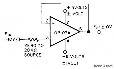
Unity-gain connec tion of Precision Monolithics 0P-07A opamp provides high accuracy (0.005% worst case) over temperature range of-55℃to + 125℃ for buffer applications for ±10 V signals.-D. Soderquist and G. Erdi, The OP-07 Ultra-Low Off-set Voltage Op Amp-a Bipolar Op Amp That Challenges Choppers, Eliminates Nulling, Precision Monolithics, Santa Clara, CA, 1975, AN13, p 8. (View)
View full Circuit Diagram | Comments | Reading(1938)
PROGRAMMABLE_AMPLIFIEIR
Published:2009/7/9 21:10:00 Author:May
Often a circuit will be called upon to perform several functions. In these situations, the variable gain configuration of this circuit could be quite useful. This programmable gain stage depends on CMOS analog switches to alter the amount of feed-back, and thereby, the gain of the stage. Placement of the switching elements inside the relatively low-current area of the feedback loop, minimizes the effects of bias currents and switch resistance on the calculated gain of the stage. Voltage spikes can occur during the switching process, resulting in temporarily reduced gain because of the makebefore-break operation of the switches. This gain loss can be minimized by providing a separate voltage divider network for each level of gain. (View)
View full Circuit Diagram | Comments | Reading(778)
PROGRAMMABLE_GAIN_DIFFERENTIAL_INPUT_AMPLIFIER
Published:2009/7/9 21:08:00 Author:May
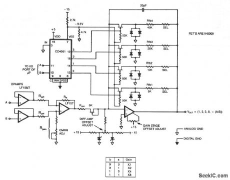
This programmable gain circuit employs a CD4051 CMOS Analog Multiplexer as a two to four line decoder, with appropriate FET drive for switching between feedback resistors to program the gain to any one of four values. (View)
View full Circuit Diagram | Comments | Reading(3037)
SMALL_CURRENT_AMPLIFIER
Published:2009/7/9 21:08:00 Author:May
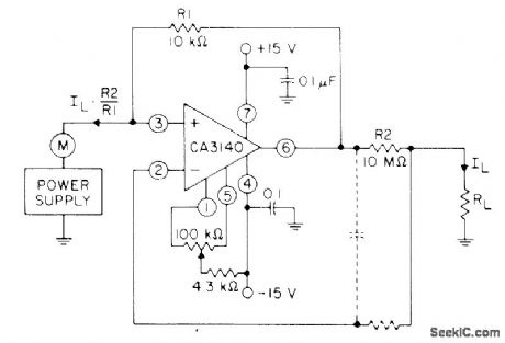
CA3140 bipolar MOS opamp serves as high-gain current amplifier. Input current through load is increased by ratio of R2 to R1, which is 1000 for values shown, for reading by meter M. Dashed lines show method of decoupling circuit from effects of high output-lead capacitance.- Circuit Ideas for RCA Linear ICs, RCA Solid State Division, Somerville, NJ, 1977, p 13. (View)
View full Circuit Diagram | Comments | Reading(976)
DIGITALLY_PROGRAMMABLE_PRECISION_AMPLIFIER
Published:2009/7/9 21:06:00 Author:May
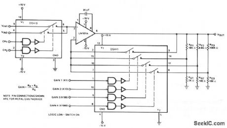
The DG419 looks into the high input impedance of the op amp, so the effects of RDS(on) are negligible.The DG441 is also connected in series with RIN and is not included in the feedback dividers, thus contributing negligible error to the overall gain. Because the DG419 and DG441 can handle ±15 V, the unity gain follower connection, X1, is capable of the full op-amp output range of ±12 V. (View)
View full Circuit Diagram | Comments | Reading(953)
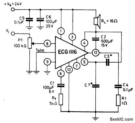
5_watt_AF_power_amplifier_with_16_ohm_load_connected_to_ground_using_no_bootstrap
Published:2009/7/20 4:15:00 Author:Jessie
5-watt AF power amplifier with 16-ohm load connected to ground using no bootstrap. The ECG1116 is a 12-pin QIP. To obtain the rated output heatsinking is required. Capacitor C3 is typically 330 pF, while C7 is 1500 pF. Generally C7 is five times greater than C3. Supply voltage ripple rejection is improved by connecting a capacitor (10 to 100 μF at 25 volts) between pin 7 and ground. Frequency response is from 40 hertz to 20 kilohertz (courtesy GTE Sylvania Incorporated). (View)
View full Circuit Diagram | Comments | Reading(939)
5_watt_AF_power_amplifier_with_16_ohm_load_connected_to_ground_and_using_bootstrap
Published:2009/7/20 4:14:00 Author:Jessie

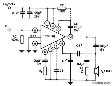
5-watt AF power amplifier with 16-ohm load connected to ground and using bootstrap. For low voltage operation (e.g., 9 to 14volts) 150 ohms is connected between pins 1 and 4. To improve power supply ripple rejection capacitor C5 (10 to 100 μF at 25 volts) is connected between pin 7 and ground. Capacitor C3 is typically 330 pF and C7 is 1500 pF. Generally C7 is five times greater than C3 Frequency response is from 40 hertz to 20 kilohertz (courtesy GTE Sylvania Incorporated). (View)
View full Circuit Diagram | Comments | Reading(668)
52_watt_AF_power_amplifier_for_automotive_applications
Published:2009/7/20 4:04:00 Author:Jessie
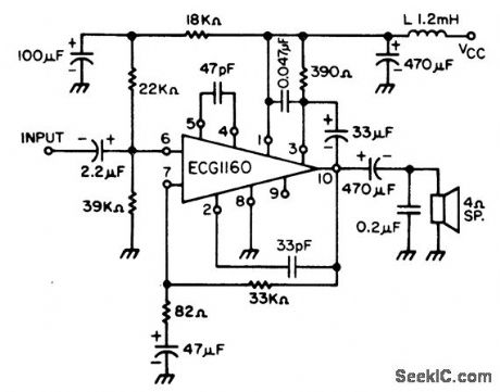
52-watt AF power amplifier for automotive applications. Recommended supply voltage is 13.2 volts. No-signal current drain is typically 28 mA. Voltage gain is 51.5 dB (courtesy GTE Sylvania Incorporated). (View)
View full Circuit Diagram | Comments | Reading(600)
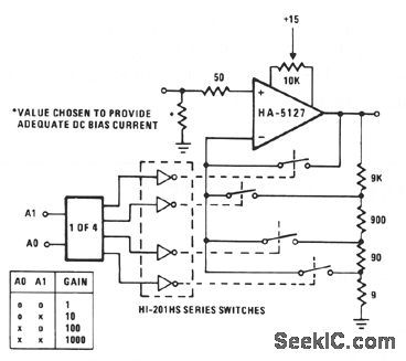
NONINVERTING_PROGRAMMABLE_GAIN_AMPLIFIER
Published:2009/7/9 21:00:00 Author:May
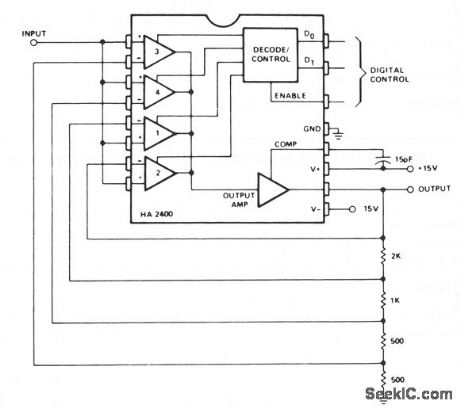
This is a noninverting amplifier configuration with feedback resistors chosen to produce a gain of 0, 1, 2, 4, or 8, depending on the digital control inputs. Comparators at the output could be used for automatic gain selection for auto-ranging meters, etc. (View)
View full Circuit Diagram | Comments | Reading(906)
INVERTING_PROGRAMMABLE_GAIN_AMPLIFIER
Published:2009/7/9 20:59:00 Author:May
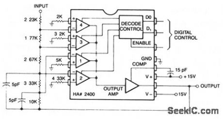
This circuit can be programmed for a gain of 0, -1, -2, -4, or -8. This could also be accom-plished with one input resistor and one feedback resistor per channel in the conventional manner, but this would require eight resistors, rather than five. (View)
View full Circuit Diagram | Comments | Reading(719)
21_watt_AF_power_amplifier_for_radio
Published:2009/7/20 3:57:00 Author:Jessie
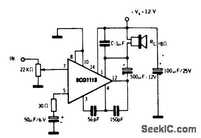
2.1-watt AF power amplifier for radio. The 2.1-watt rating is for an 8-ohm load. The ECG1113 is a 14-pin QIP. Recommended supply voltage is 12 volts, which makes it ideal for automotive applications. Current drain at maximum output is 235 mA. Typical voltage gain is 70 dB (courtesy GTE Sylvania Incorporated). (View)
View full Circuit Diagram | Comments | Reading(754)
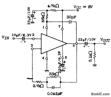
33_watt_AF_power_amplifier_using_an_ECG1118
Published:2009/7/20 3:56:00 Author:Jessie
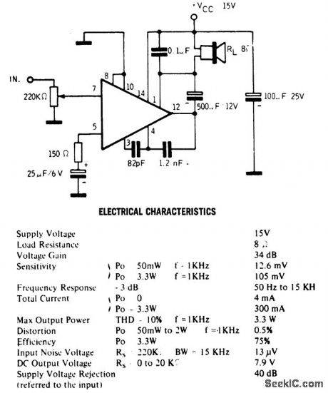
3.3-watt AF power amplifier using an ECG1118. This circuit is intended for phonograph applications (courtesy GTE Sylvania Incorporated). (View)
View full Circuit Diagram | Comments | Reading(656)
| Pages:99/250 At 2081828384858687888990919293949596979899100Under 20 |
Circuit Categories
power supply circuit
Amplifier Circuit
Basic Circuit
LED and Light Circuit
Sensor Circuit
Signal Processing
Electrical Equipment Circuit
Control Circuit
Remote Control Circuit
A/D-D/A Converter Circuit
Audio Circuit
Measuring and Test Circuit
Communication Circuit
Computer-Related Circuit
555 Circuit
Automotive Circuit
Repairing Circuit