
Amplifier Circuit
Index 65
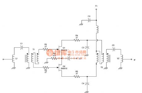
the oscillator circuit of the radio frequency :LP Pierce oscillator RF circuit
Published:2011/8/13 0:32:00 Author:Ariel Wang | Keyword: oscillator, LP , Pierce
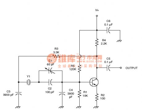
View full Circuit Diagram | Comments | Reading(791)
the oscillator circuit of the radio frequency :Pierce oscillator RF circuit
Published:2011/8/13 0:34:00 Author:Ariel Wang | Keyword: oscillator, Pierce, RF
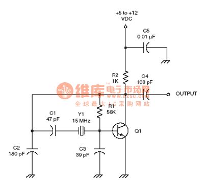
View full Circuit Diagram | Comments | Reading(1087)
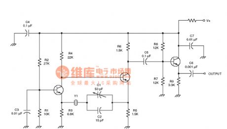
the oscillator circuit of the radio frequency :Tuned Miller oscillator RF circuit
Published:2011/8/13 1:00:00 Author:Ariel Wang | Keyword: oscillator, radio frequency , tuned, miller
View full Circuit Diagram | Comments | Reading(1326)
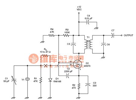
the Oscillator circuit of the radio frequency :Buffered Butler oscillator RF circuit
Published:2011/8/12 22:05:00 Author:Ariel Wang | Keyword: Oscillator, radio frequency , Buffered, Butler
View full Circuit Diagram | Comments | Reading(1541)
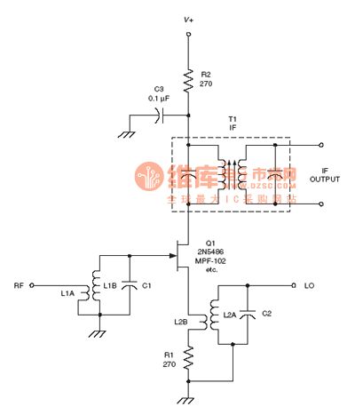
the mixer circuit of the radio frequency :Dual JFET mixer RF circuit
Published:2011/8/12 21:40:00 Author:Ariel Wang | Keyword: Mixer, radio frequency , Dual , JFET
View full Circuit Diagram | Comments | Reading(1763)
the Mixer circuit of the radio frequency :Dual MOSFET mixer RF circuit
Published:2011/8/12 22:00:00 Author:Ariel Wang | Keyword: Mixer, Dual, MOSFET, RF
View full Circuit Diagram | Comments | Reading(697)
the mixer circuit of the radio frequency :JFET mixer RF circuit
Published:2011/8/12 22:01:00 Author:Ariel Wang | Keyword: mixer, RF, JFET
View full Circuit Diagram | Comments | Reading(2706)
DC tachometer generator and single chip microcomputer interface circuit
Published:2011/7/20 7:07:00 Author:Fiona | Keyword: DC tachometer generator, single chip microcomputer, interface
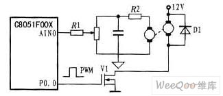
Figure is DC tachometer generator and single chip microcomputer interface circuit.In this system,it produces the PWM signal through the single chip microcomputer mouth to control the rotate speed of DC tachometer generator.Adding DC tachometer generator at the shaft of DC generator is used for measuring the motor's rotate speed,the tachometer generator output is analogue value,so it must A / D convert the output signal into digital tachometer signal,the tachometer signal compares with the given PWM signal through single chip microcomputer,it is used for acceleration or deceleration,thus forms the motor's closed-loop control system.
(View)
View full Circuit Diagram | Comments | Reading(795)
Diagram of Electronic Ballast Circuit composed of UBA2014
Published:2011/8/9 18:05:00 Author:Vicky | Keyword: Electronic Ballast
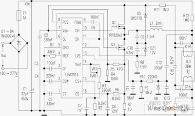
36W electronic ballast circuit diagram is shown in the above picture. When the power supply AC is on, it can charge capacitance C2 in the pin VDD of UBA2014 via the current of resistances R12 and R11. When the voltage of C2 rises to 13V, VCO inside the oscillator begins vibrating, and half-bridge power level composed by Q1 and Q2 generates output. When the oscillator begins working, the frequency is fmax=100kHz, and then it soon goes down to preheat frequency fpn. The preheat time is determined by R1 and R5. When R1 equals 33kΩ, and C5 equals 330nF, the preheat time tph equals 1.8 seconds. Once the preheat is over, the output frequency of ballast goes down again. During this procession, series circuit LC composed by output ends L1 and C15 begins vibrating, and then a high-voltage pulse is generated in the ends of C15, which goes through the light tube and then ignites. The frequency of oscillator reduces to fmin=40kHz. (View)
View full Circuit Diagram | Comments | Reading(3270)
RK609 Single-chip Microcomputer Control Integrated Circuit
Published:2011/8/3 7:31:00 Author:Michel | Keyword: Single-chip, Microcomputer Control, Integrated Circuit
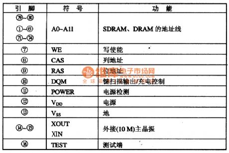
RK609 is the chip microcomputer control integrated circuit that is widely used in TCL, WanLiDa, JinZheng reapter etc.
First,Functions Features
RK609 intergrates CPU, D/A, A/D conversion and LCD display , the input analog signal converts into digital signals via IC , then it is stored in the deposit.
Second,Pins Functions and Data are shown as table 1.RK609 IC pins functions are shown as table 1.
Table 1:RK609 IC Pins Functions (View)
View full Circuit Diagram | Comments | Reading(700)
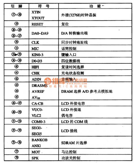
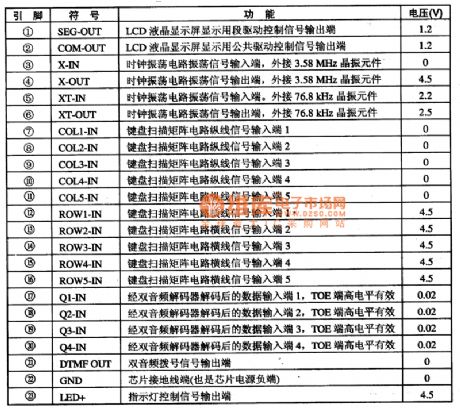
P5346003 Communication Monolithic Microcomputer Integrated Circuit
Published:2011/8/3 7:11:00 Author:Michel | Keyword: Communication, Monolithic Microcomputer, Integrated Circuit
'
P5346003 is a communication single-chip microcomputer integrated circuit and it is widely used in caller id telephone.
First,Functions FeatureS346003 integrated circuit internal basically contains the following functions: FSK circuit frequency shift keying decoder (the decoder is according with BlLL202 and ITU-TV23 standard). LCD drive and control circuit can directly drive LCD screen.A frequency signal generator DTMF, which can achieve a frequency dial-up and the audio signal output controlled by software.The battery is low voltage detection circuit: software control energy saving mode control circuit.
Second,Pins Functions and DataP5346003 integrated circuits uses 30 feet encapsulation, and it is directly sealed in the printed circuit board.It is a kind of four microcomputer and the integrated circuit pins functions are shown as table 1.
Table 1:Microprocessor P5346003 IC Pins and Data (View)
View full Circuit Diagram | Comments | Reading(686)
PCMl710U 2O Double Track DAC Integrated Circuit
Published:2011/8/3 7:09:00 Author:Michel | Keyword: Double Track, DAC Integrated Circuit
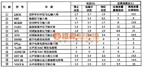
PCMI7I0U is the D/A converter integrated circuits produced by the BB company and it is widely used in VCD, SVCD, DVD, VCD audio D/A transformation.
First,Functions Features
PCMl710U integrated circuit contains eight times sampling digital filter and 4 order noise plastic circuit. It uses many △-∑ structure and level 5 conversion level.They are not sensitive to time setting jitter and power supply fluctuation. There is simulation low pass filter, which can simplify an external circuit of the design.And the failure rate drops greatly.
Second,Pins Functions and Data
PCM1710U integrated circuit uses feet 28 DIP package and its pins functions and data is shown as table 1.
Table 1 :PCMl710U IC Pins Functions and Data (View)
View full Circuit Diagram | Comments | Reading(760)
PCD4421 Microcomputer Dialing Integrated Circuit
Published:2011/8/3 7:05:00 Author:Michel | Keyword: Microcomputer Dialing, Integrated Circuit
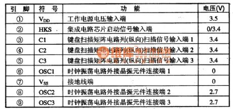
PCD4421 is the microcomputer dial-up integrated circuit produced by Dutch philips company and it is used in communication equipment and dial-up circuit.
PCD4421 integrated circuit containins a number of frequent generating circuit, R key control circuit, the keyboard switch circuit and noise control decoding static circuit etc. This IC adopts feet 18 DIP package and the pins functions and data are shown as table 1.
Table 1:Pins Fuctions and Data ofPCD4421 IC (View)
View full Circuit Diagram | Comments | Reading(653)
Comparator Circuit of TL431
Published:2011/8/3 7:04:00 Author:Michel | Keyword: Comparator Circuit
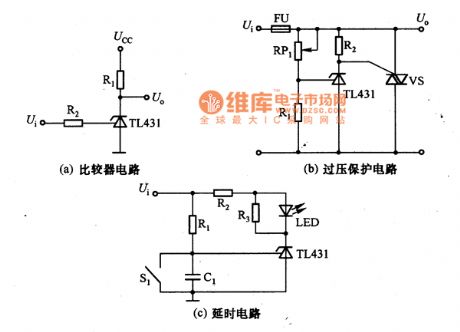
The picture a,b,c are comparator circuits of TL431.The picture (a) is comparator circuit of TL431.When input voltag9be Ui≥2.5V,the output voltage U。=2V;Ui<2.5V,the output U。=Ucc.
The picture (b) is protection voltage of TL431.When input voltage Ui exceeds 1+RRP1/R1)UREF, a larger current flows through the fuse,FU burns out to achieve the purpose of voltage protection.The picture (c) is delay circuit of TL431,the voltage on C1 is zero,TL431 stops and LED does not shine.With C1 charging voltage rises,TL431 conducts, LED displays by shining.The delay time(from input voltage to LED shining)is R1C1ln[Ui/(Ui-UREF)].S1 is reset switch, when it is connected,C1 discharges and prepares for the next delay. (View)
View full Circuit Diagram | Comments | Reading(3637)
SDA6000 System Control Microcomputer Integrated Circuit
Published:2011/8/3 7:30:00 Author:Michel | Keyword: Microcomputer, Integrated Circuit
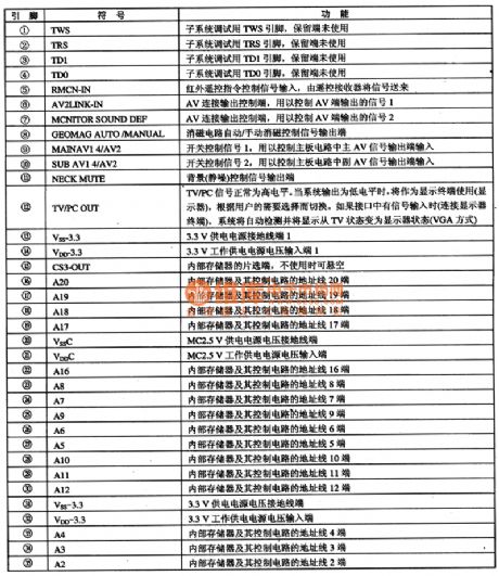
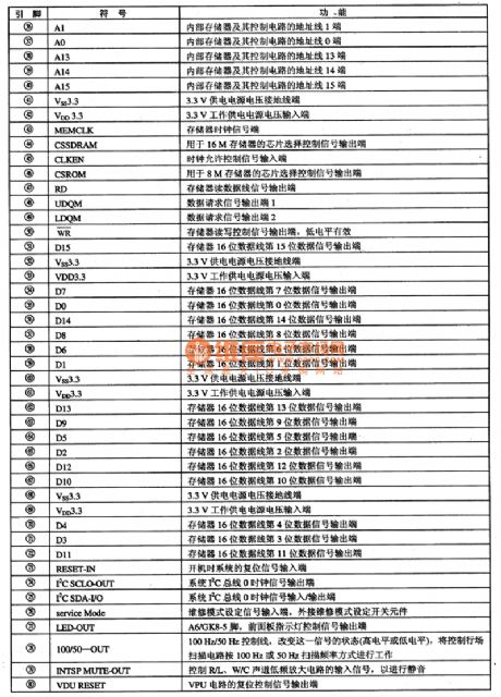
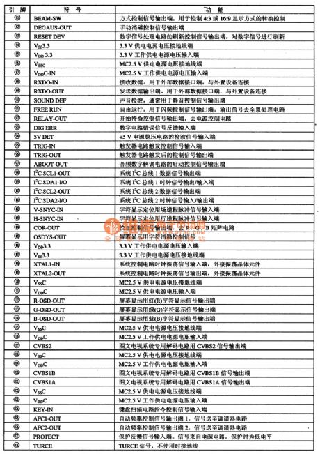
SDA6000 is a new type system control microcomputer integrated circuit that is widely used in EURO7 and GIGAP5O0 series big screen color TV of Panasonic.
First,Functions and Features
SDA6000 integrated circuit has two pieces of the usual memory chips, one is 8M rapid FLASH memory (a FLASH) solid ROMR read memory and it is used in system of data read.The other one is the 16M SDRAM conventional memory (RAM). This configuration storage capacity is much larger than the average color TV set, and can fully satisfy completing new function needs of the multi-function large screen color TV.
Second,Pins FunctionsSDA6000 integrated circuit uses 128 feet square structure and its pins functions are shown as table 1.
Table 1:SDA6000 IC Pins Functions and Data (View)
View full Circuit Diagram | Comments | Reading(752)
Infrared Control Telephone Code Lock Circuit
Published:2011/8/1 0:31:00 Author:Michel | Keyword: Infrared Control, Telephone Code Lock
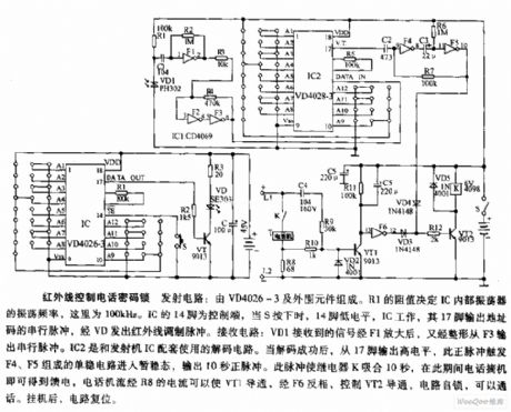
The infrared control telephone code lock emitting circuit is composed of VD4026-3 and peripheral components. R1 resistance value decides the IC internal oscillator oscillation frequency, here it's 100 KHz.IC 14 feet is control circuit.14 feet outputs low PWL and 17 feet outputs address serial pulse and launches infared adjusting pulse when S is pressed.Receiving circuit:VD1 receiving signal is amplifiedvia F1 and it's surged and then it outputs serial pulse via F3.IC2 is decoding circuit of transmitter IC.When the decoding is finished successfully,high PWL is output from 17 feet,the positive pulse makes F4 and F5 monostable circuit enter transition state and it outputs 10s positive pulsr and the pulse make relay K actuate 10 S.
(View)
View full Circuit Diagram | Comments | Reading(746)
The circuit of DC inverting amplifier whose gain is decided by the ratio
Published:2011/7/27 8:24:00 Author:Fiona | Keyword: DC reversed-phase amplifier
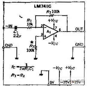
Circuit WorkBecause the OP amplifier inverting input is grounded, inverting input in the linear operating range is zero level. So the input resistance of the circuit is R1, if R2 remains unchanged, the input resistance decreased with the increased gain. Due to there has input bias current IB flowing through in the OP amplifier, if removing the resistance R3, it will produce additional bias. If you are using FET input type OP amplifier, you can save R3.
Because the magnification is 10 times,the circuitneeds toincrease the offset adjustment circuit, in the 741-type OP amplifier, the circuit connects the 10 k ohms variable resistor between 1,5 lead.
(View)
View full Circuit Diagram | Comments | Reading(770)
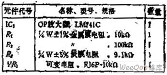
The AC inverting amplifier circuit that maintain bias by the selected gain
Published:2011/7/27 8:22:00 Author:Fiona | Keyword: selected gain, AC inverting amplifier, maintain bias
Circuit function
Dispense with amplified DC signal, it is in series with a blocking capacitor C1 at the input resistance,it can make the offset drift neglected. Even though the AC gain of amplifier is high, the output is still DC working, OP amplifier is only used as a simple amplification devices. Using R3 = R2 to achieve input current bias, but because of the DC gain L, therefore, this requirement is not too strict, such as the resistance of R2 is small, R2 can be removed. Increasing the capacitor C1, it can get low-frequency time constant, the frequency F0 is 1 / N, C1.R1, phase shift is 45 degrees, characteristic curve downs 1 / √ 2 (3DB). Therefore, to obtain flat characteristics, it should be in accordance with FO(1 / 3 ~ 1 / 5) to determine the C1 value.
(View)
View full Circuit Diagram | Comments | Reading(773)
2 W x 2 power amplifier(LM1877)circuit
Published:2011/8/8 9:07:00 Author:Fiona | Keyword: 2 W x 2 power amplifier
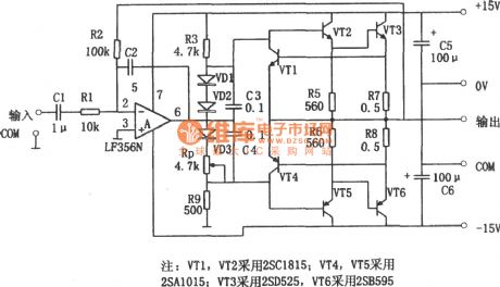
Shown in the figure,the circuituses on,under symmetrical structure and has two way signal which is added respectively to the two op-amp non-inverting input ends of LM1877,its output end’s external way is same with the input end: it uses 2.7 Ω resistor and 0.1 u F to form the high frequency filter circuit to prevent the high frequency of self-excited; coupling capacitor Co (470 u F) and load resistor ZL (loudspeaker:8Ω) concert the output power into voice to output, and the magnitude of Co and ZL circuit is also determined to the circuit’s lower-cut-off frequency fL,the relationship between this three is: fL=1/(2πZLCo),corresponding to the parameters in the figure,its fL = 42 Hz.
(View)
View full Circuit Diagram | Comments | Reading(1552)
Touch Biostable Controller Circuit
Published:2011/8/2 1:30:00 Author:Joyce | Keyword: Touch , Biostable , Controller
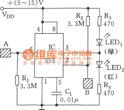
Feet 6 and 2 of 555 are connected with the inphase and inverse input ends of comparator A1 and A2 within the substrate respectively to control its state of reset and set to change its output state. Touching metal A will reset 555, and LED (green) will be enlightened and LED1 (red) will go out; Touching metal 8 will enlighten LED2 and quench LED1 . If the relay is changed over, the control of on-off of power supply for the executive circuit can be achieved.
(View)
View full Circuit Diagram | Comments | Reading(954)
| Pages:65/250 At 206162636465666768697071727374757677787980Under 20 |
Circuit Categories
power supply circuit
Amplifier Circuit
Basic Circuit
LED and Light Circuit
Sensor Circuit
Signal Processing
Electrical Equipment Circuit
Control Circuit
Remote Control Circuit
A/D-D/A Converter Circuit
Audio Circuit
Measuring and Test Circuit
Communication Circuit
Computer-Related Circuit
555 Circuit
Automotive Circuit
Repairing Circuit