
Amplifier Circuit
Index 74
HAMMER_DRIVER_FOR_COMPUTER_LINE_PRINTER
Published:2009/7/15 23:23:00 Author:Jessie
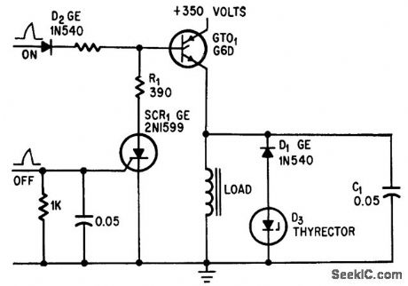
Gale turnoff scr overdrives load solenoid momentarily by connecting it across 350-v bus and disconnecting before over heating occurs. Load current rise and fall limes are less than one millisec.-D. R. Grafham, Now the Gale Turnoff Switch Speeds Up D-C Switching, Electronics, 37:12, p 64-71. (View)
View full Circuit Diagram | Comments | Reading(813)
COAXIAL_CABLE_DRIVER
Published:2009/7/15 23:21:00 Author:Jessie
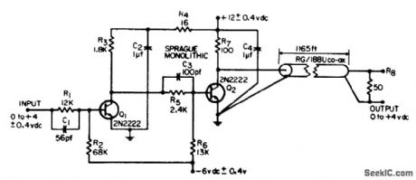
Can drive digital information through long lengths of coaxial cable. Will send pulses with 30-nsec rise and fall time through 1,155 feet of 50-ohm RG/ 188U or through 650 feet of 93-ohm RG/ 62U.-B. Strunk, Coaxial Cable Driver Circuit, EEE, 13:5, p 43-44. (View)
View full Circuit Diagram | Comments | Reading(2157)
1200_W_PEP_POWER_AMPLIFIER
Published:2009/7/14 2:00:00 Author:May
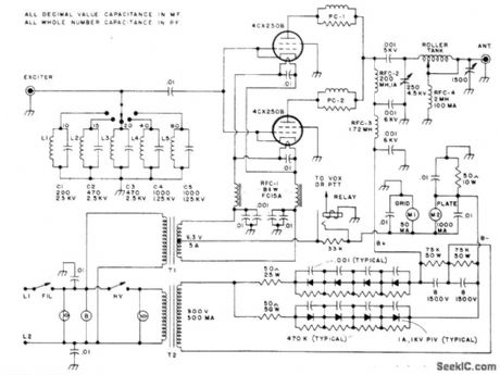
Ceramic tetrodes are operated as low-mu triodes, with control grids tied to cathodes. Amplifier takes about 200-W drive. Tuned-cathode input circuit presents better load to exciter. Bias is developed through 33K cathode resistor that is shorted out by relay during operation. In standby mode, plate current is virtually zero. Article covers construction and operation, with emphasis on proper cooling of tubes. Separate tuned circuits are required for each amateur band. L1 and L2 are 0.15 μH, L3 and L4 are 0.31 μH, and L5 is 1.3 μH. PC-1 and PC-2 are 3 turns No. 16 enamel wound on 50-ohm 2-W carbon resistor-S. W. Hochman, The Ample Amplifier, 73Magazine, March 1973, p 50-54. (View)
View full Circuit Diagram | Comments | Reading(8289)
100_KV_FOR_ACCELERATOR
Published:2009/7/15 22:41:00 Author:Jessie
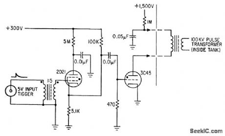
Two thyrcttrons trigger pulse amplifier to send 1,500-v pulse to primary of pulse transformer for step up to l00 kv for Van de Graaff accelerator source. -E. J. Rogers, Van de Graaff Proton Source Receives 1l0 Kilovolt Boosts, Electronics, 35:13, p 58-59. (View)
View full Circuit Diagram | Comments | Reading(1451)
TWO_AMPLIFIERS_FOR_BIPOLAR_PULSES
Published:2009/7/15 22:38:00 Author:Jessie
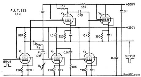
Design procedure is based on fact that wide bandwidth is required only for leading and trailing edges of pulses. Auxiliary amplifier supplies current to charge load and stray capacitances, reducing standby current and improving gain. Auxiliary amplifier V4.VS provides charging current for shunt capacitance during positive-going edge of output pulse.-J. F. Golding, Novel Approach to Pulse Amplifier Design, Electronics, 33:1, p 64-66. (View)
View full Circuit Diagram | Comments | Reading(665)
WIDEBAND_DIGITAL_PULSE_AMPLIFIER
Published:2009/7/15 22:37:00 Author:Jessie
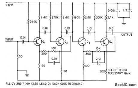
Common-emitter ac coupled cascaded amplifiers, with negative feedback at every second stage, give voltage gain of 12, bandwidth of 100 Mc, rise time of 3 nsec, pulse pair resolution of 5 nsec, and s/n ratio of 100 to1 for inputs from 0 to 200 my.-A. A. Fleischer and E. Johnson, New Digital Conversion Method Provides Nanosecond Resolution, Electronics, 36:18, p 55-57. (View)
View full Circuit Diagram | Comments | Reading(1142)
BUFFER
Published:2009/7/14 1:25:00 Author:May
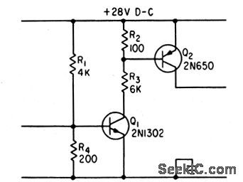
Used between ring counters when readout number has several digits, to make final stage of one counter fire first stage of next counter while resetting first counter.-F. W. Kear, Digital Control Uses Unijunction Transistors, Electronics, 34:18, p 79-80. (View)
View full Circuit Diagram | Comments | Reading(931)
FUNCTION_GENERATOR_POWER_BUFFER
Published:2009/7/14 1:18:00 Author:May
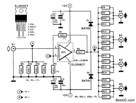
This buffer circuit can be used as an output booster for any function generator that has to be extended in order to drive several loads. The heart of the circuit is a video distribution amplifier IC from Elantec, the EL2099CT (listed by RS Components). This interesting device has a 3-dB power bandwidth of no less than 65 MHz at a gain of x2. Here, it is used to drive up to four 50-Ω loads at a maximum signal level in excess of 10 Vpeak. When used for video applications, the EL2099CT can drive up to six 75-Ω loads. The gain of the amplifier is x2; unity gain is not possible because of instability problems. The bandwidth of the circuit shown here is >10 MHz, while the output achieves a drive margin of >10 Vpeak . Current consumption will be of the order of 200 mA. (View)
View full Circuit Diagram | Comments | Reading(5398)
NONVOLATILE_LATCH
Published:2009/7/14 1:00:00 Author:May
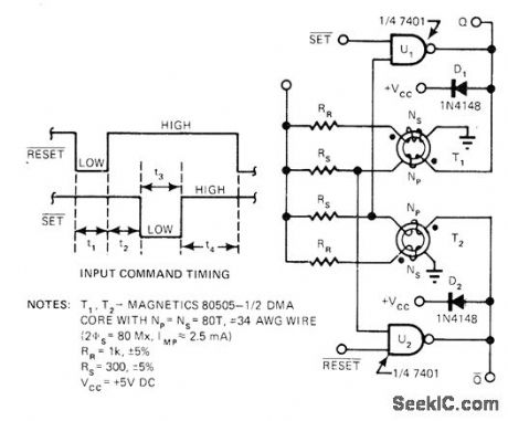
Design shown for latch gives immunity to interfering noise pulses on command line and prevents loss of essential data bit during unexpected power-line interruption. Subminiature saturable transformers in positive feedback paths between two gates of latch prevent instantaneous change of state. Transformers remain magnetically biased in positive or negative saturation even without circuit power, to provide pretransient-state reference to which latch must return when power is reapplied.-G. E. Bloom, Add Nonvolatility to Your Next Latch Design, EDN Magazine, Jan. 5, 1978, p 80 and 82. (View)
View full Circuit Diagram | Comments | Reading(980)
SWITCHING__SINGLE_SUPPLY_OPAMPS
Published:2009/7/14 0:58:00 Author:May
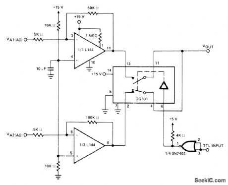
DG301 low-power analog switch serves as interface between TTL control input and DC-coupled opamp pair Logic level determines which opamp is connected to single output.- Analog Switches and Their Applications, Siliconix, Santa Clara, CA, 1976, p 7-88-7-89. (View)
View full Circuit Diagram | Comments | Reading(883)
MIXER_LOAD_DIFFERENTIAL_AMPLIFIER
Published:2009/7/15 23:25:00 Author:Jessie
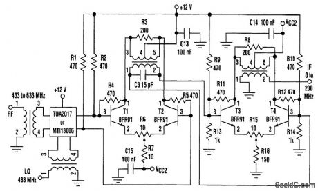
Two different amplifier stages are used as the load of the mixer TUA2017 or MTl13006 (products developed by Siemens Co.). The LQ frequency is fixed at 483 MHz, because a commercial SAW oscillator at 483 MHz can be used as a local oscillator. If the RF frequency is swept from 433 to 633 MHz, then the IF frequency also is swept from 0 to 200 MHz. Compared to a passively loaded mixer, this combination of mixer and differential amplifiers exhibits excellent performance. The relative amplitude (amplitude difference between the fundamental frequency and the largest distortion frequency) is typically at least 50 dB. But it is only 30 dB (or less) in the case of a passive load mixer. Resistors R4, R5, R11, and R12 are used as the shunt feedback to obtain the flat output amplitude when the RE frequency is swept. The amplitude ripple with the IF bandwidth (0 to 200 MHz) is less than 0.5 dB. (View)
View full Circuit Diagram | Comments | Reading(1077)
SWITCHING_OPAMP
Published:2009/7/14 0:53:00 Author:May
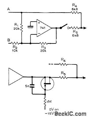
Circuit provides change-over function when only single pair of contacts is available. With switch open, input A goes to output. With switch closed, input B goes to out-put and signal of input A is inverted by opamp so as to cancel direct signal A. Gain is unity for both output signals. Switch can be replaced by FET as in lower diagram; here, capacitor pre vents FET from cutting off during positive half-cycle above about 100 Hz. In multichangeover applications, opamp could be section of programmable opamp.-M. J. Sells, Electronic Changeover Switching, Wireless World, Dec.1974, p 503. (View)
View full Circuit Diagram | Comments | Reading(930)
READ_WRITE_AMPLIFIER
Published:2009/7/16 1:33:00 Author:Jessie
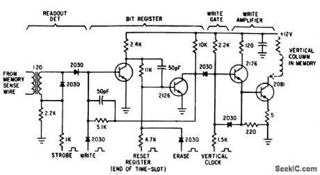
Each of 28 vertical circuits for coincident-flux memory consists of readout detector, bit register (flip-flop), write gate, and two-stage write amplifier-H. F. Priebe, Jr., Three-Hole Cores for Coincident.Flux Memory, Electronics, 33:31, p 94-97. (View)
View full Circuit Diagram | Comments | Reading(698)
OUTPUT_CONTROL_FOR_CLOCK_COMPARATOR
Published:2009/7/13 22:45:00 Author:May
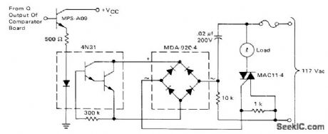
Circuit triggers 10-A triac when Q output of comparator-driven flip-flop is logic 1. LED in optoisolator is then energized, activating phototransistor pair for driving gate circuit of triac through diode bridge. Trigger voltage of triac is positive for first quadrant and negative for third quadrant, to give maximum sensitivity of triac control.-D. Aldridge and A. Mouton, Industrial Clock/Timor Featuring Back-Up Power Supply Operation,” Motorola, Phoenix, AZ, 1974, AN-718A, p 7. (View)
View full Circuit Diagram | Comments | Reading(1543)
POWER_OPAMP_FOR_CONTROL
Published:2009/7/13 22:29:00 Author:May
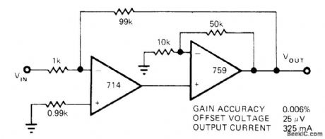
Precision 714 opamp drives 759 power opamp to give ultraprecision power amplifier system. High current capability (up to 500-mA peak output current) makes circuit suitable for such control applications as driving motors, relays, solenoids, or transmission lines. Article tells how to calculate heatsink requirements for opamp.-R. J. Apfel, Power Op Amps-Their Innovative Circuits and Packaging Provide Designers with More Options, EDN Magazine, Sept. 5, 1977, p 141-144. (View)
View full Circuit Diagram | Comments | Reading(1621)
SEISMIC_RADIO_BEACONAUDIO_VCO_AND_BUFFER
Published:2009/7/13 22:25:00 Author:May
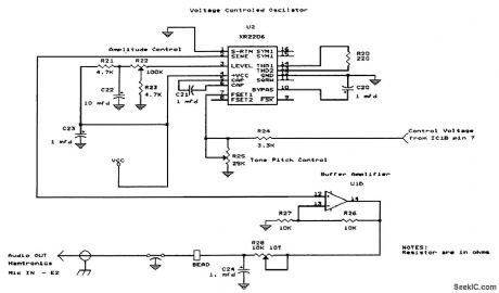
This audio and VCO buffer is fed by a geophone amplifier and produces a tone modulated by seismic activity, as picked up by a geophone. (View)
View full Circuit Diagram | Comments | Reading(1443)
4224_MHz_POWER_AMPLIFIER
Published:2009/7/13 21:44:00 Author:May
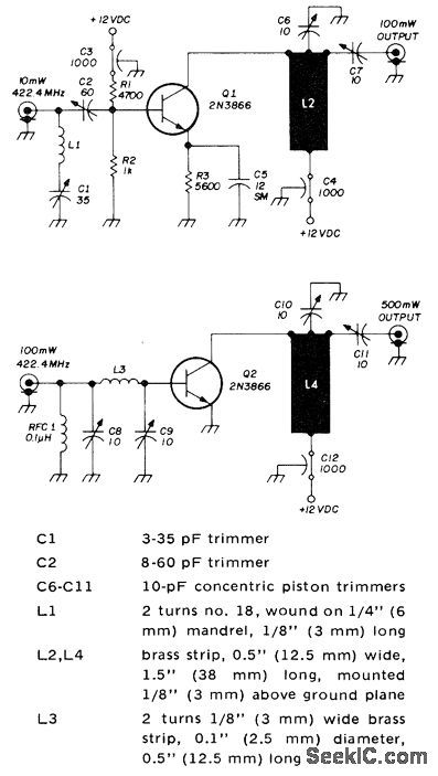
Used in local oscillator chain of 1296-MHz SSB transceiver to boost 10-mW output of chain to 500 mW as required for driving final diode-type tripler stage. Sections are connected together with miniature 50-ohm coax.-H. P. Shuch, Easy-to-Build SSB Transceiver for 1296 MHz, Ham Radio, Sept. 1974, p 8-23.
(View)
View full Circuit Diagram | Comments | Reading(962)
45_MC_CASCODE_FET
Published:2009/7/16 2:38:00 Author:Jessie
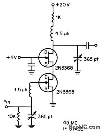
Operates without neutralization, giving 20 db power gain and 6-Mc bandwidth. -Cascode with FET's (Siliconix ad), Electronics, 39:2, p 109. (View)
View full Circuit Diagram | Comments | Reading(1028)
SINGLE_TUNED_FINAL_I_F
Published:2009/7/16 2:33:00 Author:Jessie
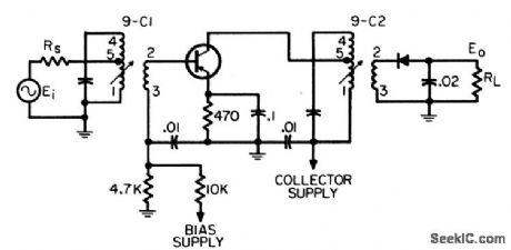
Circuit is example of optimum design based on use of transistor signal-handling curves. Transformers are single-tuned.-W. Rheinfelder, Using transistor Signal Handling Curves in Receiver Design, EEE, 14:6, p 62-66. (View)
View full Circuit Diagram | Comments | Reading(759)
OPTIMIZED_LOW_DISTORTION_I_F_AMPLIFIER
Published:2009/7/16 2:32:00 Author:Jessie
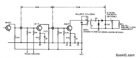
Provides 0.5 V audio from detector, with 3 db of control with agc. Volume control is diode detector load resistor. First i-f stage uses ceramic filters for sharper bandpass characteristic.-W. Rheinfelder, Using Transistor Signal Handling Curves in Receiver Design, EEE, 14:6, p 62.66. (View)
View full Circuit Diagram | Comments | Reading(834)
| Pages:74/250 At 206162636465666768697071727374757677787980Under 20 |
Circuit Categories
power supply circuit
Amplifier Circuit
Basic Circuit
LED and Light Circuit
Sensor Circuit
Signal Processing
Electrical Equipment Circuit
Control Circuit
Remote Control Circuit
A/D-D/A Converter Circuit
Audio Circuit
Measuring and Test Circuit
Communication Circuit
Computer-Related Circuit
555 Circuit
Automotive Circuit
Repairing Circuit