
Amplifier Circuit
Index 70
30_4000_Hz_WITH_OPAMP
Published:2009/7/15 2:35:00 Author:Jessie
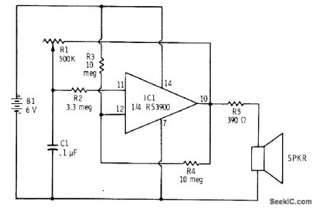
Frequency is determined by pot R1 in feedback path. Square-wave output pulse amplitude is about 5 V. Circuit will generate almost perfect sine waves if 0.1-μF capacitor is connected between pin 12 and ground; R1 must be properly adjusted to give output of about 220 Hz. - F. M. Mims,″Integrated Circuit Projects, Vol. 6,″Radio Shack, Fort Worth,TX,1977, p 89-95. (View)
View full Circuit Diagram | Comments | Reading(837)
DARLINGTON_AMPLIFIER
Published:2009/7/15 2:34:00 Author:Jessie
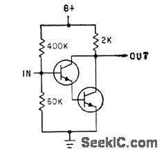
Useful up to 100 kc, but high input impedance makes it particularly desirable for audio preamps. Gives gain of two stages with dissipation of only one.-L. Pollock and R. Gutteridge, Latest Design Techniques for Linear Microcircuits, Electronics, 35:41, p 47-49. (View)
View full Circuit Diagram | Comments | Reading(1209)
25_W_CLASS_B_POWER_AMPLIFIER
Published:2009/7/15 2:31:00 Author:Jessie
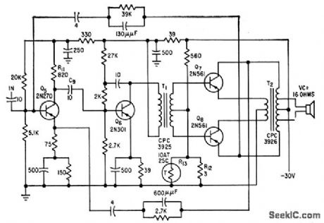
Uses balanced negative feedback, with input Q5 and driver Q6 operating class A.Output stage is temperature-stabilized.-R. Minton, Designing High-Quality A-F Transistor Amplifiers, Electronics, 32:24, p 60-61. (View)
View full Circuit Diagram | Comments | Reading(1073)
FOUR_SPEED_PLAYBACK_PREAMP
Published:2009/7/14 7:28:00 Author:May
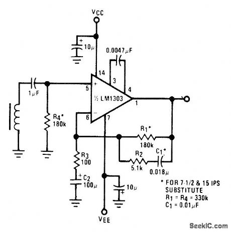
Provides 0-dB reference gain of 34 dB. Supply can be ±4.5 to ±15 V. Values shown are for NAB equalization and 1 7/8 or 3 3/4 in/s; for 7 1/2 and 15 in/s, change values as indicated. Design equations are given.- Audio Handbook, National Semiconductor, Santa Clara, CA, 1977, p 2-31-2-37. (View)
View full Circuit Diagram | Comments | Reading(1159)
LOGARITHMIC_INPUT_CURRENI_COMPRESSOR
Published:2009/7/14 6:07:00 Author:May
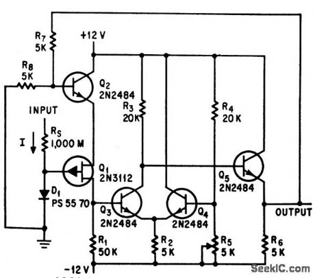
Simple d-c logarithmic amplifier compresses positive input current into logarithmically related input voltage.-G. W. Candel, D-c Logarithmic Amplifier Compresses Input Current, Electronics, 39:10, p91-92. (View)
View full Circuit Diagram | Comments | Reading(860)
LOW_DRIFT_WITHOUT_CHOPPER
Published:2009/7/14 6:05:00 Author:May
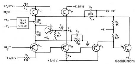
Developed for airborne or missile telemetry. Gain is adjustable. Has wide frequency response, high common-mode rejection factor, and high input impedance, along with gain stability of 0.15% over wide temperature range.-R. D Middlebrook and A. D. Taylor, Differential Amplifier with Regulator Achieves High Stability, Low Drift, Electronics, 34:30, p 56-59. (View)
View full Circuit Diagram | Comments | Reading(786)
CALIBRATED_GAIN_AMPLIFIER
Published:2009/7/15 2:21:00 Author:Jessie
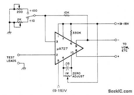
Used to extend low range of VOM or CRO and provide very high input impedance (above 1000 megohms), Gain of amplifier from DC up to several hundred kilohertz is determined by ratio of 10K feedback resistor to 200- or 2000- ohm preset pot. Action is noninverting Maximum input voltage range is ±10V Dual battery supply must be used To calibrate, short input test leads and adjust 1-megohm pot for zero on VOM or other indicating instrument.-J. J. Schultz, Versatile Test Equipment Range Extender, 73 Magazine,Nov 1973, p 59-62. (View)
View full Circuit Diagram | Comments | Reading(672)
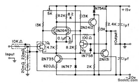
FET_UNITY_GAIN_D_C_AMPLIFIER
Published:2009/7/14 5:54:00 Author:May
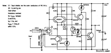
Each base of 2N2641 dual transistor is driven by source follower fet’s Q1 and Q2. Q1 performs impedance transformation, while Q2 closes feedback loop and tends to cancel changes in parameters due to temperature variations.-L. J. Sevin, Jr. Field-Effect Transistors, McGraw-Hill, N.Y.1965, p102. (View)
View full Circuit Diagram | Comments | Reading(909)
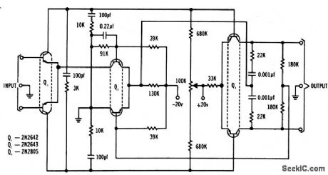
UNITY_GAIN_TEMPERATURE_STABLE_D_C_AMPLIFIER
Published:2009/7/14 5:52:00 Author:May
Two bootstrapped cathode followers are combined to form differential input stage, where one gate serves as feedback input and other as signal input. Field effect transistors Q1 and Q2 are matched.-Texas In-struments Inc., Solid-State Communications, McGraw-Hill, N.Y.1966, p139. (View)
View full Circuit Diagram | Comments | Reading(854)
COMPLEMENTARY_PAIR_LOW_LEVEL
Published:2009/7/14 5:50:00 Author:May
Dual transistors provide extremely high gain, to give greater stability with fewer stages. Circuit has low drift and high common-mode rejection (120 db) for either differential or single-ended outputs. Differential input impedance is 500K minimum, gain-bandwidth product is 5Mc, and low-frequency voltage gain is 68 db.-Texas Instruments Inc Solid-Slate Communications, McGraw-Hill,N.Y.1966, p290. (View)
View full Circuit Diagram | Comments | Reading(897)
MULTISTAGE_PROGRAMMABLE_AMPLIFIER
Published:2009/7/14 4:42:00 Author:May
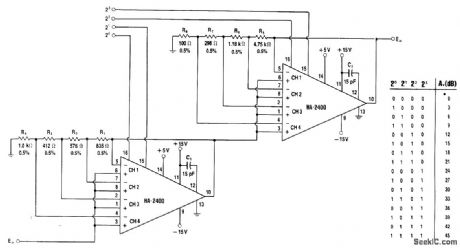
Cascading of two HA-2400 four-channel programmable amplifiers gives choice of 16 different values of gain, ranging from 0 to 45 dB, by applying logic pulses to control inputs for pins 15 and 16 in accordance with truth table shown.-W. G. Jung, IC Op-Amp Cookbook, Howard W. Sams, Indianapolis, IN, 1974, p 433-435. (View)
View full Circuit Diagram | Comments | Reading(1005)
MOS_FET_AMPLIFIER
Published:2009/7/15 2:10:00 Author:Jessie
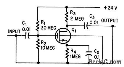
Circuit draws only 6 microamp while providing voltage gain over200.-G. G. Luettgenau and S.H. Barnes, Designing With Low-Noise MOS FETs: A LittleDifferent But No Harder, Electronics, 37:31, p 53-58. (View)
View full Circuit Diagram | Comments | Reading(1053)
UNDERWATER_PREAMPLIFIER
Published:2009/7/15 2:09:00 Author:Jessie
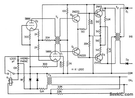
Used in package with hydrophone for measuring ambient oceannoise over periods of months, as one basis for sonar system design. Output is fedthrough cable pair to shore installation.-J.V. Schaefer, Remote Preamplifiers forUnder Ocean Work, Electronics, 33:28, p 60-62. (View)
View full Circuit Diagram | Comments | Reading(799)
MICROPHONE_PREAMP
Published:2009/7/14 5:35:00 Author:May
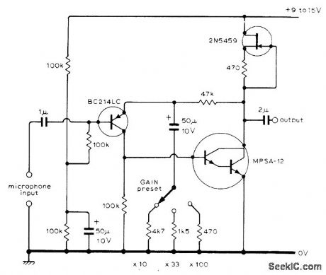
Used in high-quality stereo cassette deck operating from AC line or battery. Provides three preset gain positions (10, 33, and 100) to meet amplification requirements of practically all types of microphones used with tape recorders. Recording input of cassette deck provides only enough gain for re-cording from audio amplifier or radio tuner delivering 50-100 mV at fairly low impedance, hence is not suitable for microphone input. Article gives all other circuits of cassette deck and describes operation in detail.-J. L. Linsley Hood, Low-Noise, Low-Cost Cassette Deck, Wireless World, Part 2-June 1976, p 62-66 (Part 1-May 1976, p 36-40; Part 3-Aug. 1976, p 55-56l. (View)
View full Circuit Diagram | Comments | Reading(1646)
PLAYBACK_PREAMP
Published:2009/7/14 5:34:00 Author:May
Circuit is optimized for automotive use at supply of 10-15V. Wideband 0-dB reference gain is 46 dB. NAB equalization is included. Tape speeds can be 1 7/8 or 3 3/4 in/s.- Audio Handbook, National Semiconductor, Santa Clara, CA, 1977, p 2-31-2-37. (View)
View full Circuit Diagram | Comments | Reading(918)
RECORDING_AMPLIFIER_1
Published:2009/7/14 5:33:00 Author:May

Designed for use with microphone having 10-mV peak output and recording head requiring 30-μA AC drive current. Output swing is 6 VRMS. High-frequency cutoff is 16 kHz, with circuit designed for slope of 6 dB per octave between 4 kHz and 16 kHz to compensate for falling frequency response of recording head starting at 4 kHz.- Audio Handbook, National Semiconductor, Santa Clara, CA, 1977, p 2-31-2-37. (View)
View full Circuit Diagram | Comments | Reading(833)
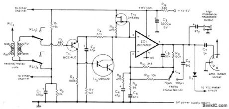
RECORDING_AMPLIFIER
Published:2009/7/14 5:32:00 Author:May
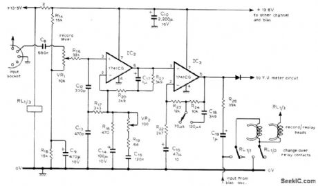
Used in high-quality stereo cassette deck operating from AC line or battery. Uses active RC circuit R16-R17-C12-C13-R19-VR2-C15 to provide required high-frequency recording characteristic for use with Garrard CT4 recording head; component values may have to be changed for other heads. C18 (3.9 nF) is switched in to change from basic 70-μs recording characteristic to 120μs. C17 and R27 provide new cassette-standard bass preemphasis at 3,180μs. Recording level is chosen as 0 VU at 660 Hz. Output feeds VU meter through silicon diode, Article gives all other circuits of cassette deck and describes operation in detail.-J. L. Linsley Hood, Low-Noise, Low-Cost Cassette Deck, Wireless World, Part 1-May 1976, p 36-40 (Part 2-June 1976, p 62-66; Part 3-Aug. 1976, p 55-56).
(View)
View full Circuit Diagram | Comments | Reading(1326)
REPLAY_AMPLIFIER
Published:2009/7/14 5:27:00 Author:May
Used in high-quality stereo cassette deck operating from AC line or battery. Amplifier design is optimized for mini-mum noise voltage by using PNP silicon input transistor operated with lowest possible collector current (10μA for Texas Instruments transistor specified). Motorola IC in second stage, similar to 741 but having 8-pin metal-can en-capsulation, provides equalization required for replay. Output of amplifier is about 0.4 VRMS. Article gives all other circuits of cassette deck and describes operation in detail.-J. L. Linsley Hood, Low-Noise, Low-Cost Cassette Deck, Wireless World, Part 1-May 1976, p 36-40 Part2-June 1976, p 62-66; Part3-Aug. 1976, p 55-561. (View)
View full Circuit Diagram | Comments | Reading(937)
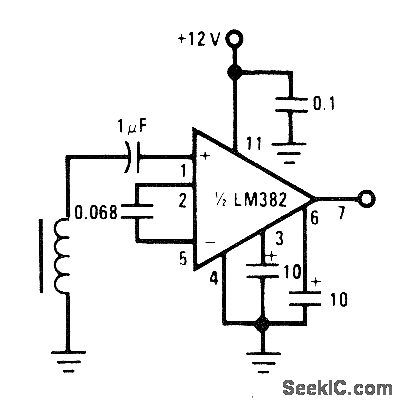
NAB_PLAYBACK_PREAMP
Published:2009/7/14 5:18:00 Author:May
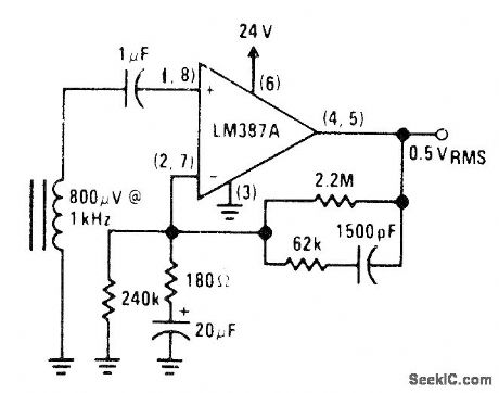
Provides standard NAB equalization for tape player requiring 0.5 VRMS from head having sensitivity of 800μV at 1 kHz, with operating speed of 3 3/4 in/s. Design procedure is given. Voltage gain at 1 kHz is 56 dB.- Audio Handbook, National Semiconductor, Santa Clara, CA, 1977, p 2-31-2-37. (View)
View full Circuit Diagram | Comments | Reading(2013)
HEADPHONE_AMPLIFIER
Published:2009/7/14 5:16:00 Author:May
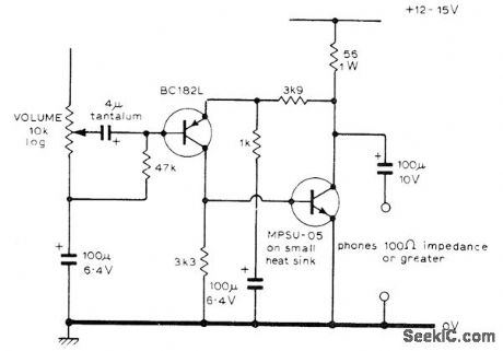
Used in high-quality stereo cassette deck operating from AC line or battery. Provides gain of 5 in class A, for use with low-sensitivity headphones or low-impedance headphones down to 100 ohms. Replay amplifier output alone is adequate for head-phones having 2000-ohm load impedance or high sensitivity. Article gives all other circuits of cassette deck and describes operation in detail. Input to volume contrails taken from output of opamp in replay amplifier, nominally about+5V.-J. L. Linsley Hood, Low-Noise, Low-Cost Cassette Deck, Wireless World, Part 2-June, 1976, p 62-66 (Part 1-May 1976, p 36-40; Part 3-Aug, 1976, p 55-56). (View)
View full Circuit Diagram | Comments | Reading(0)
| Pages:70/250 At 206162636465666768697071727374757677787980Under 20 |
Circuit Categories
power supply circuit
Amplifier Circuit
Basic Circuit
LED and Light Circuit
Sensor Circuit
Signal Processing
Electrical Equipment Circuit
Control Circuit
Remote Control Circuit
A/D-D/A Converter Circuit
Audio Circuit
Measuring and Test Circuit
Communication Circuit
Computer-Related Circuit
555 Circuit
Automotive Circuit
Repairing Circuit