
Communication Circuit
Index 22
GENERAL_PURPOSE_IR_RECEIVER
Published:2009/6/19 4:18:00 Author:May
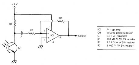
Suitable for amplitude-modulated IR beams, this receiver provides an audio signal that corresponds to the modulation envelope. Phototransistor Q1 should be properly mounted and shielded from stray light. This receiver should drive a small earphone dire (View)
View full Circuit Diagram | Comments | Reading(2561)
FM_INFRARED_RECEIVER_FOR_AUDIO_RECEPTION
Published:2009/6/19 4:17:00 Author:May
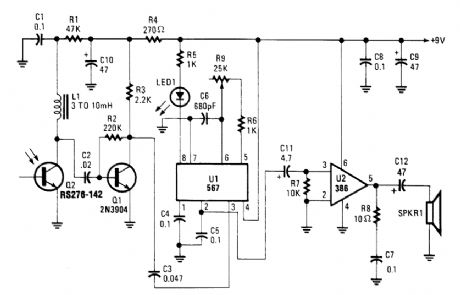
Modulated IR energy strikes Q2, a phototransistor. Q1 is a tunde amplifier,and feeds PLL detector U1.U2 is an audio amplifier that drives a speaker. (View)
View full Circuit Diagram | Comments | Reading(1007)
Call display circuit diagram
Published:2011/7/14 22:24:00 Author:zj | Keyword: Call display circuit
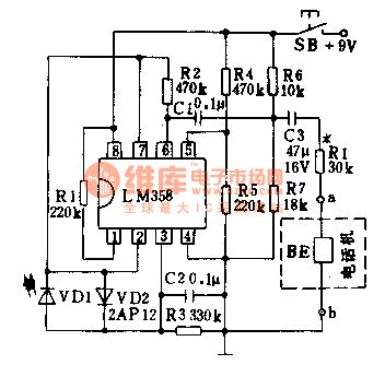
LEDcan automatically display various function afterpicking up the machine. It is used to display the working state of the telephone. For the reason that it adopts a integration technology, the circuit has the advantages of small volume, high reliability, less external components, convenient assembly, low power consumption and low cost.Work principleis as shown in Figure 143. When you pick up the machinethe key switch STL closes. Integrated operational amplifying circuit LM%8's pin6 andpin0 willrecieve 9V DC voltage. (View)
View full Circuit Diagram | Comments | Reading(878)
DOPPLER_ULTRASOUND_TRANSMITTER
Published:2009/6/19 4:12:00 Author:May
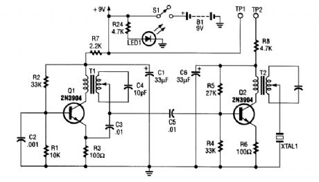
The 2.25-MHz oscillator Q1 drives amplifier Q2 and XTAL1, an ultrasonic transducer. The trans-ducer is a lead zirconate-titanate type. Taps on T1 and T2 provide low-impedance drive points. (View)
View full Circuit Diagram | Comments | Reading(1501)
LOW_POWER_INFRARED_DATA_LINK_RECEIVER
Published:2009/6/19 4:11:00 Author:May
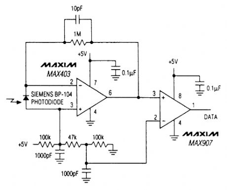
The Maxim MAX403 in this circuit consumes only 1 mA and is capable of speeds over 1 MBPS. (View)
View full Circuit Diagram | Comments | Reading(858)
AUDIO_MODULATED_IR_TRANSMITTER
Published:2009/6/19 4:00:00 Author:May
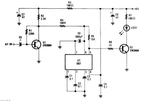
This circuit produces an effect similar to frequency modulation (FM) by varying the voltage at pin 6 of the PLL using an audio signal. The FM 1R signal can be picked up by a receiver with an FM detector suitably tuned. (View)
View full Circuit Diagram | Comments | Reading(1216)
FM_RADIO_TRANSMITTER
Published:2009/6/19 4:00:00 Author:May
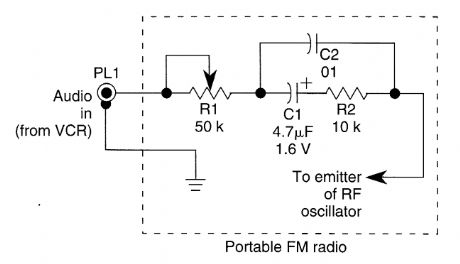
An FM radio generates an interference signal that can be picked up on another FM radio tuned 10.7 MHz above the first one. The 50-kΩ potentiometer adjusts the modulation level to maximum without distortion. The RC network improves the fidelity of the transmitted signal and provides dc isolation. The component values shown are provided as a starting point. They can vary somewhat for clifferent radios. Note that if you can't get the signal at 10.7 MHz above the frequency setting of the first radio, try tuning at 10.7 MHz below. Also, note that both tuned frequencies must be unused.Otherwise, you will hear your audio on top of the audio that is already there. You might have to play with both frequencies until you find two blank spots that are l0.7 MHz apart. (View)
View full Circuit Diagram | Comments | Reading(909)
LOW_POWER_40_METER_CW_TRANSMITTER_
Published:2009/6/19 3:59:00 Author:May
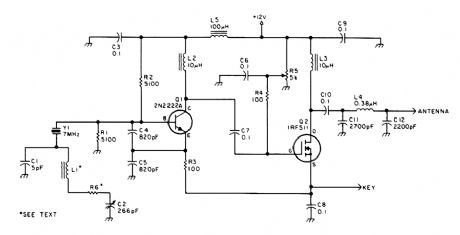
This CW transmitter has an output of up to 3 W. By using 24 V on Q2, up to 10 W output can be obtained. If a 24-V supply is used, Q1 must not see more than 12 V. Connect 12Vbetween junctions C3, R2 and L2, and remove L5. L1 should be a low-Q 18- to 20-μH inductor. R6 can be used (up to 47 Ω) to reduce the Q further. (View)
View full Circuit Diagram | Comments | Reading(2409)
1O_METER_DSB_TRANSMITTER
Published:2009/6/19 3:54:00 Author:May
A DSB transmitter is much cheaper to build than an SSB transmitter because no filter or phasing networks are required. This circuit produces up to 1-W output on the 10-meter band. The frequency 28.322 MHz is used, which is a commonly available clock frequency crystal. CW operation is also provided. A doubly balanced mixer assembly is used as a modulator and CW keyer (View)
View full Circuit Diagram | Comments | Reading(2029)
1750_METER_TRANSVERTER
Published:2009/6/19 3:46:00 Author:May
This circuit was described in a recent edition of an amateur radio magazine. It allows operation in the 160- to 190-kHz band with up to 1 W (license free) in any mode (CW/SSB/FM, etc.). It consists of a receiving converter for 5 kHz to 450 kHz and a transmitting converter to convert the 3.66- to 3.69-MHz (80 meter) range to 160 to 190 kHz. A 12- to 24-V power supply can be used. (View)
View full Circuit Diagram | Comments | Reading(1363)
EXPERIMENTAL_FIBER_OPTIC_DATA_RECEIVER
Published:2009/6/19 1:47:00 Author:May
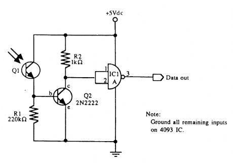
An infrared phototransistor acts as the sensor for this recelver IC1a is a section of a CD4093 CMOS NAND gate. (View)
View full Circuit Diagram | Comments | Reading(1747)
EXPERIMENTAL_DATA_TRANSMITTER_FOR_FIBER_OPTICS
Published:2009/6/19 1:45:00 Author:May
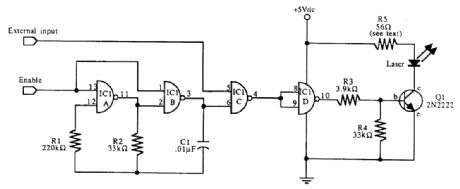
This schematic for an experimental data transmitter uses optical fibers and a laser diode. Trans-mission frequency of the free-running oscillator is approximately 3 kHz. R5 might have to be varied to suit your laser diode. IC1 is a CD4093. (View)
View full Circuit Diagram | Comments | Reading(2318)
CRYSTAL_CONTROLLED_FM_STEREO_TRANSMITTER
Published:2009/6/19 1:37:00 Author:May
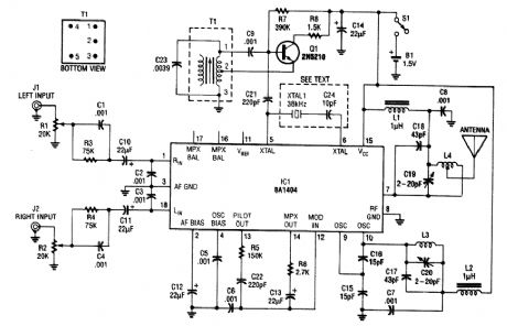
In this application, a BA1404 is used to generate an FM MPX baseband signal. This modulates a crystal oscillator (Q3) via a dual varactor series modulator. This transmitter can be to play CD audio on an existing FM auto radio. (View)
View full Circuit Diagram | Comments | Reading(2985)
DMAl2 Main schematic circuit diagram
Published:2011/4/24 22:28:00 Author:muriel | Keyword: schematic circuit diagram
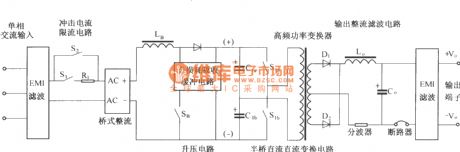
The figure shows a simplified schematic diagram of main circuit DMA12. It is mainly composed of input circuit and electromagnetic interference (EMI) filter circuit, impulse current limit circuit, the input rectifier filter circuit, the boost / power factor correction circuit and the absorption circuit, half-bridge power translation circuit, the output rectifier filter circuit. Compared with the DMA10, DMA12 uses single-phase input, boost/power factor correction method and lossless to absorb the buffer circuit, and the half-bridge DC / DC power conversion and output rectification filter part is the same with the DMA10.
(View)
View full Circuit Diagram | Comments | Reading(2040)
FM_STEREO_TRANSMITTER
Published:2009/6/18 23:44:00 Author:May
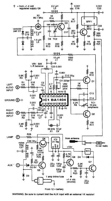
A BA1404 IC is used to generate a complete FM MPX signal. The chip contains all of the necessary circuitry. C1 and R3, and R4 and C4 provide pre-emphasis. The transmitter runs on a single AA cell. L3 is 3 tums of #20 wire on a 3/6 drill (for a form). L3 is1/4 long. L4 is 4 turns #20 wire on 3/6 drill bit, spaced to 3/8 . If monophonic operation is wanted, omit C5 and the 38-kHz oscillator components. (View)
View full Circuit Diagram | Comments | Reading(312)
SPEECH_SCRAMBLER
Published:2009/6/18 22:37:00 Author:May
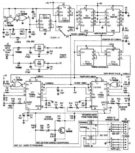
Using digital techniques, this circuit accomplishes the frequency-inversion algorithm via digiti-zation of the audio, inversion of the sign of every alternate sample, and D/A conversion of the resul-tant data. The result is an inverted frequency spectrum. Because the circuit has two channels, this system can be used in a full duplex two-way telephone scrambler.A complete kit ofparts is available from North Country Radio, PO. Box 53, Wykagyl Station, New Rochelle, NY 10804-0053A. (View)
View full Circuit Diagram | Comments | Reading(1241)
VOICE_IDENTIFIER_FOR_HAM_RADIO_USE
Published:2009/6/18 22:27:00 Author:May
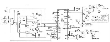
Using an ISD1016 audio record/playback chip (Information Storage Devices, Inc.), this circuit records and plays back mes-sages on command. Although intended for use with transmitters, it can be used as an electronic notepad, etc. Consult the ISD1016 data sheet for other applications. (View)
View full Circuit Diagram | Comments | Reading(2610)
QRP_TRANSCEIVER_FOR_18,21,AND_24_MHz
Published:2009/6/18 5:40:00 Author:May
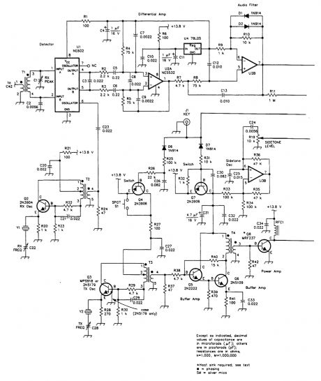
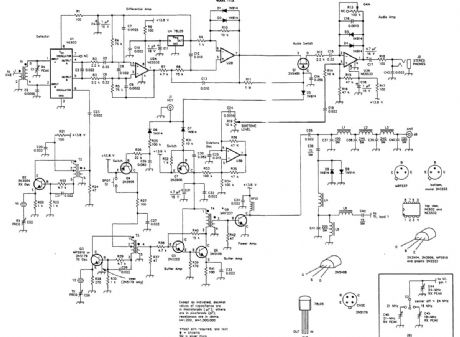
This CW transceiver has 1.25 to 4 W RF output, a direct-conversion receiver, full break-in, and SW sidetone generation.The power supply is 13.8 V, which makes this transceiver suitable for mobile or portable operation. (View)
View full Circuit Diagram | Comments | Reading(3491)
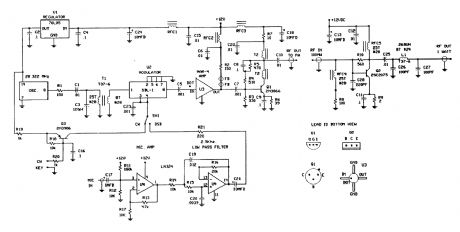
49_MHz_FM_TRANSMITTER
Published:2009/6/18 5:22:00 Author:May
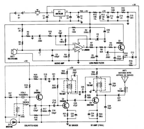
This 49-MHz FM transmitter consists of an audio amplifier, a low-pass filter, three RF stages, and a regulated-dc power supply. The output is about 16 mW into a 50-Ω load. This transmitter can be used in many 49-MHz applications, such as in a baby monitor, cordless telephone, or in conjunction with a scanner as a one-way voice link. (View)
View full Circuit Diagram | Comments | Reading(3204)
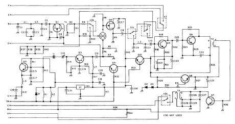
TRACKING_TRANSMITTER
Published:2009/6/18 5:15:00 Author:May
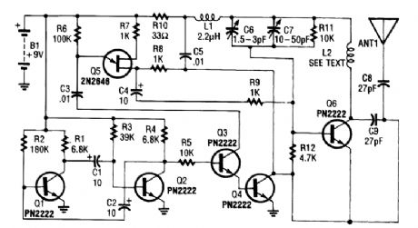
This tracking transmitter consists of four distinct subassemblies; a free-running multivibrator, a transmit switch, an audio-tone generator, and an FM transmitter. The multivibrator (which produces a pulse width with a pulse separation of 1500 ms) is built around Q1 and Q2. The multivibrator out-put is coupled through R5 to the base of Q3, whose emitter feeds Q4, which controls the circuit's transmitter section. (View)
View full Circuit Diagram | Comments | Reading(286)
| Pages:22/32 At 20212223242526272829303132 |
Circuit Categories
power supply circuit
Amplifier Circuit
Basic Circuit
LED and Light Circuit
Sensor Circuit
Signal Processing
Electrical Equipment Circuit
Control Circuit
Remote Control Circuit
A/D-D/A Converter Circuit
Audio Circuit
Measuring and Test Circuit
Communication Circuit
Computer-Related Circuit
555 Circuit
Automotive Circuit
Repairing Circuit