
Communication Circuit
Index 23
VACUUM_TUBE_LOW_POWER_80_40_METER_TRANSMITTER
Published:2009/6/18 5:12:00 Author:May
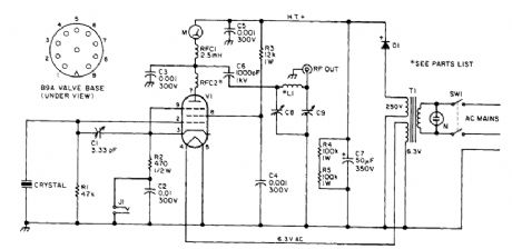
Using a 6BW6 vacuum tube, the above transmitter delivers about 5 W output. C1 is adjusted for cleanest CW note. C8 and C9 are 365 pF and dual-365 pF (paralleled) tuning capacitors. L1 is 35 turns of #24 enamelled wire on a 1 plastic tube. FT-243 crystals for 3.5 or 7-MHz are used. Do not use this circuit to produce a 7-MHz output from a 3.5-MHz crystal-it is not intended to double over crystal frequencies. (View)
View full Circuit Diagram | Comments | Reading(2805)
SIMPLE_FM_TRANSMITTER
Published:2009/6/18 5:08:00 Author:May
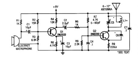
Running from a 9-V battery, this transmitter can be used as a wireless rrticrophone with an ordi-nary 88- to 108-MHz FM broadcast receiver. Keep the antenna length under 12 inches to comply with FCC limits. L1 is 6 tums of #24 wire wound around a pencil or a 1/4 form, with tums spaced I wire diameter. C6 is a gimmick capacitor of about 1 pF. (View)
View full Circuit Diagram | Comments | Reading(682)
6_W_ECONOMY_MORSE_CODE_TRANSMITTER_FOR_7_MHz
Published:2009/6/18 5:06:00 Author:May
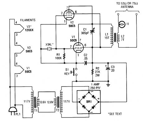
The vacuum tube is still alive and useful in some applications, as in this CW transmitter. The circuit was built in old-fashioned breadboard style on a wooden base. Old table radios are a good source of parts for this circuit. V3 is used as a ballast resistor-a 75-Ω, or 100-Ω 5-W resistor could be sub-stituted. L1 is 15 turns of hookup wire on a 7/8 form 2 long. L2 is 7 turns of the same wire. L2 is wound over L1. Be careful as up to 160 V is present on VI and V2. (View)
View full Circuit Diagram | Comments | Reading(1598)
ATV_JR_TRANSMITTER_440_MHz
Published:2009/6/18 5:00:00 Author:May
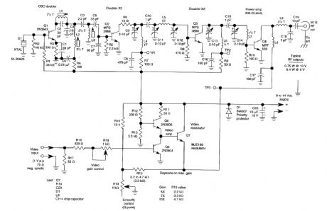
This low-power video transmitter is useful for R/C applications, surveillance, or amateur radio applications. Seven transistors are used in a crystal oscillator multiplier RF power amplifier chain, and a high-level video modulator. A 9-to 14-Vdc supply is required. Output is 0.4 to 1.2 W, depending on supply voltage. A complete kit of parts is available from North Country Radio, P.O.Box 53, Wykagyl Station, NewRochelle, NY 10804-00530 (View)
View full Circuit Diagram | Comments | Reading(4626)
10_M_DSB_QRP_TRANSMITTER_WITH_VFO
Published:2009/6/18 4:48:00 Author:May
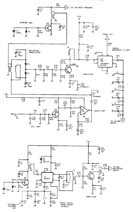
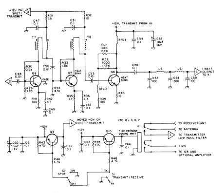
The three schematics represent three building blocks for a 10-meter SSB transmitter. Or these blocks can be used separately as circuit modules for other transmitters. The VFO board uses an FET transmittal oscillator, the VFO signal is mixed in an NE602 mixer and is amplified by Q2 to a level suf-ficient to drive an SBL-1 mixer in the transmit mixer stage (+7 to +10 dBm). In the balance mixer/modulator board, an 11-MHz crystal oscillator drives a diode balanced mixer. Audio for mod-ulation purposes is also fed to this mixer. The DSB signal feeds a 28-MHz BPR The 1-W amplifier board consists of a 3-stage amplifier and transmit/receive switching circuitry. (View)
View full Circuit Diagram | Comments | Reading(10110)
80_METER_SSB_RECEIVER
Published:2009/6/18 2:55:00 Author:May
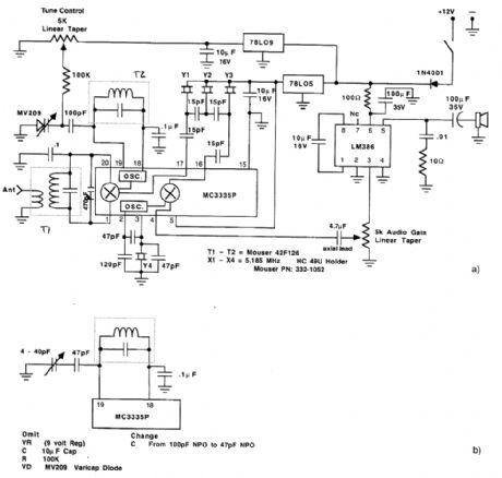
This circuit uses an MC3335P IF chip and features a 3-pole crystal filter made from microprocessor crystals. Tuning is done either with a varactor diode or air-variable capacitor, as shown.Values are for 80 meters. (View)
View full Circuit Diagram | Comments | Reading(1629)
IMPROVED_CW_TRANSMITTER_KEYING_CIRCUIT
Published:2009/6/18 2:32:00 Author:May


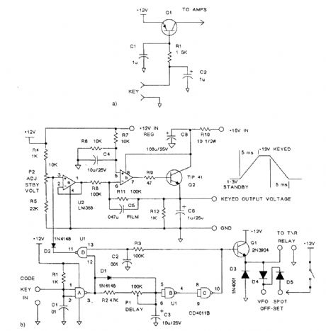
Typical (A) QRP keying circuit; (B) Improved QRP keying circuit with CMOS T/R keying control.Op amp U2b is a basic inverting amplifier with a gain of one. The capacitor C5 across the feedback resistor R11 makes it an integrator. The RC time constant of Rll and C5 determine the ramp time.The values shown will produce a 5-ms ramp. Use a good-quality capacitor for C5, such as a mylar or polypropylene type. A power transistor is placed inside the feedback loop so that the circuit can sup-ply several hundred milliamperes of current. Control P2 sets the stand-by output voltage as seen atthe emitter of Q1. U2a buffers the voltage from P2. This isolates the pot from the input of the inte-grator. With the key up, adjust the pot until you just start to see an output from your transmitter, then back it off a little. Typically, this will be between 2 and 4 V. Your output signal will now have the proper 5-ms leading and falling edges and there will be no delay between key closure and the start of the output signal.You must supply the op amp and collector of Q2 with at least 15 V to produce a full 12-V output on the emitter.Parts listR1,R4,R12 1kΩ1/4W C1 0.01μFdiskR2 47 kΩ1/4W C2 0.001μf' diskR3, R8, R11 100 kΩ C3, C4 10μF, 25VelectrolyticR6, R7 22 kΩC5 0.047μF poly-film typeR9 47Ω C6 1μF, 25 V electrolyticR10 10Ω C7 SkippedP1100 kΩ or 500 kQ trimpot C8 100 pF, 26 \I electrolyticP210 kΩ trimpot D1, D2 1N4148 diodeD3, D4, D5 1N4001 1-A diodeQ1 2N3904 NPNQ2 Tip 41-to-220 NPNU1 4011B CM0S NAND gatesU2 LM358 dual op amp (View)
View full Circuit Diagram | Comments | Reading(1482)
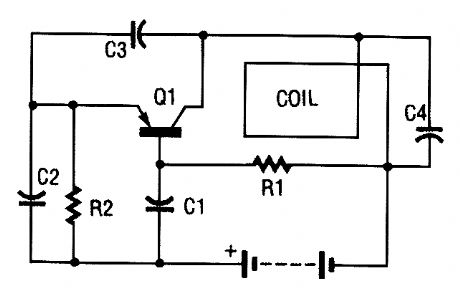
dc_to_dc_CONVERTER
Published:2009/6/18 2:26:00 Author:May
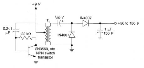
This converter should be useful where a few milliamperes of dc at a higher voltage than available supplies can deliver is needed. T1 is typically a 1 kΩ CT:10-kΩ transistor audio transformer. De-pending on T1, about 50 to 150 Vdc can be obtained at a few milliamperes. (View)
View full Circuit Diagram | Comments | Reading(111)
ISOLATED_dc_to_dc_CONVERTER
Published:2009/6/18 2:24:00 Author:May
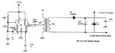

A NE555 timer is used to drive a small transformer to change the 5- to T-Vp-p output of the NE555 to a suitable value to drive a rectifier/Zener combination. This method is useful where a small isolated power source is needed. (View)
View full Circuit Diagram | Comments | Reading(3201)
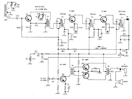
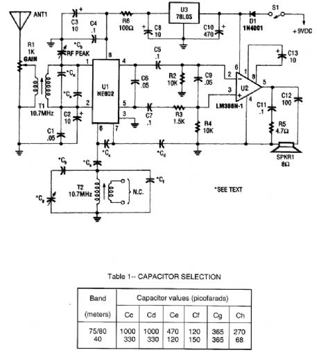
FOUR_STAGE_75_METER_SSB_SUPERHET_RECEIVER
Published:2009/6/18 2:12:00 Author:May
A simple superhet receiver for SSB reception in the 75-meter amateur band is shown.Y1 acts as a crystal filter. (View)
View full Circuit Diagram | Comments | Reading(3002)
AUTO_SECURITY_SYSTEM_RECEIVER
Published:2009/6/17 23:28:00 Author:May
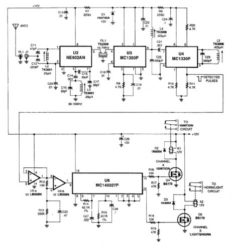
This receiver is a superheterodyne type tuned to 49 MHz. U2 is a mixer, followed by a 10.7-MHz filter and two-stage IF (U3, U4) and detector. The encoded received RE pulse signal from the an-tenna produces detected pulse from the MC1330P. These pulses are arrtplified by U5 and fed to de-coder IC U6, and MC1450278. Two channels are available at the output, which drives K1 and K2.
(View)
View full Circuit Diagram | Comments | Reading(1995)
ULTRASONIC_REMOTE_CONTROL_RECEIVER
Published:2009/6/17 23:10:00 Author:May

A GC Electronics P/N J4-815 transducer is used to receive nals. The receiver drives a relay for control of another circuit. (View)
View full Circuit Diagram | Comments | Reading(913)
METAL_LOCATOR
Published:2009/6/17 22:34:00 Author:May
The metal locator uses a one-transistor oscillator and an AM radio to detect metal. Transistor Q1 is a pnp transistor that is connected to an oscillator. Resistor RI provides the correct base bias and capacitors C3 and C4 and the search coil determine the frequency of oscillation.Capacitors C3 and C4 are fixed in value, but the search coil is an inductor that varies in induc-tance (and thus varies the oscillator frequency) as metal is brought near it. The oscillator frequency is rich in harmonics and its output falls within the AM broadcast band. The metal detector works by combining its output with the local oscillator of the AM radio. The resulting net output of the radio is a low-frequency audio tone that changes-gets higher or lower-as metal is brought near or taken away from the search coil. Commercial metal detectors use two oscillators, so they don't require an AM radio. This metal locator provides an inexpensive alternative to an expensive commercial metal locator.
C1,C2 0.01-μF Capacitor (103)C3,C4 0.001-μF CapacitorQ1 2N3906 TransistorR1 47-kΩ ResistorR2 100-Ω Resistor (View)
View full Circuit Diagram | Comments | Reading(1)
NE6O2_SUPERHET_FRONT_END
Published:2009/6/17 22:34:00 Author:May
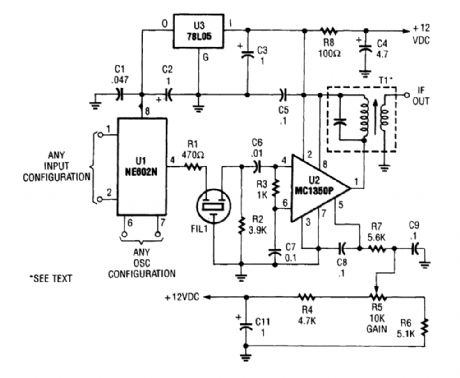
By using an NE602 with a filter and an MC1350P IC, a front end and an IF system for a basic su-perheterodyne receiver can be built with few parts. T is any suitable IF transformer for 262 kHz, 455 kHz, 10.7 MHz, etc. (View)
View full Circuit Diagram | Comments | Reading(2082)
TRANSISTORIZED_AM_RADIO
Published:2009/6/17 22:32:00 Author:May
Shown is a schematic of a typical transistor AM radio. This circuit uses npn transistors. The circuit is generic; therefore, no specific values are given for some components. This circuit is for ref-erence, to serve as a starting point for experimenters. (View)
View full Circuit Diagram | Comments | Reading(4637)
SUPER_SIMPLE_SHORTWAVE_RECEIVER
Published:2009/6/17 22:31:00 Author:May
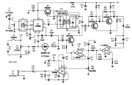
Integrated circuit U1 (an NE602 double-balanced mixer) is a combination oscillator and frequency mixer. Signals from the antenna input (at J1) are fed through dc-blocking capacitor C1 to the RF-gain control, R1, and fed to the input of U1 at pins 1 and 2.The local-oscillator frequency, which varies with the settings of R2 and L2, is mixed internally within U1, resulting in an output. The ntixer output at pin 4 of U1 is applied to a tunable 260-kHz band-pass intermediate-frequency (IF) transformer, L3, through dc-blocking capacitor C7. There-fore, signals that are roughly 260 kHz above and below the local-oscillator frequency are passed while others are effectively blocked. The IF frequencies are now amplified by Q2 and Q3. The AM au-dio signal is detected by D2 and its associated components, which bypass the RE signals, and leave only the audio signals. The signals are preamplified by U1-a (half of an LM358 dual op amp). The audio is then boosted to speaker level by the LM386low-voltage audio power amplifier, U3. (View)
View full Circuit Diagram | Comments | Reading(5328)
NE602_RF_INPUT_CIRCUITS
Published:2009/6/17 22:17:00 Author:May
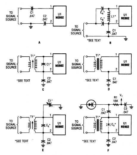
Here are a few of the many possible RE input circuits for the NE602. Just about any tuned or broadband circuit will work. (View)
View full Circuit Diagram | Comments | Reading(1197)
NE6O2_DIRECT_CONVERSION_RECEIVER
Published:2009/6/17 22:13:00 Author:May
An NEC602 is used as a mixer with a zero IF frequency output. U2 acts as an audio amplifier. This receiver is primarily for SSB and CW signals. T1 and T2 are 10.7-MHz IF coils used in AM/FM transistorized radios, etc. or in any similar indicator. (View)
View full Circuit Diagram | Comments | Reading(1817)
SIMPLE_15_V_AM_BROADCAST_RECEIVER
Published:2009/6/17 22:08:00 Author:May
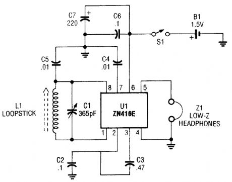
This recelver uses the ZN416E made by GEC Plessey.The tuningis via C1. (View)
View full Circuit Diagram | Comments | Reading(1155)
27145_MHz_NBFM_RECEIVER
Published:2009/6/17 22:04:00 Author:May
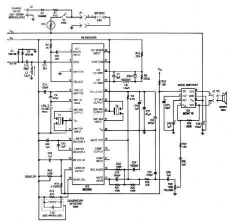
Using a Motorola MC3363 LSI one-chip FM receiver, the circuit is a dual-conversion FM receiver with a 10.7-MHz IF chain. IC4 provides power to drive a small speaker. (View)
View full Circuit Diagram | Comments | Reading(2661)
| Pages:23/32 At 20212223242526272829303132 |
Circuit Categories
power supply circuit
Amplifier Circuit
Basic Circuit
LED and Light Circuit
Sensor Circuit
Signal Processing
Electrical Equipment Circuit
Control Circuit
Remote Control Circuit
A/D-D/A Converter Circuit
Audio Circuit
Measuring and Test Circuit
Communication Circuit
Computer-Related Circuit
555 Circuit
Automotive Circuit
Repairing Circuit