
Index 280
Network voltage fault protection indication circuit
Published:2011/4/22 19:15:00 Author:Nicole | Keyword: network voltage, fault protection
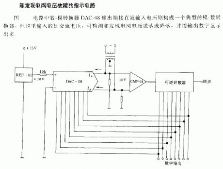
The circuit is as shown, the ouput termlnal of digital-analog converter DAC-08 connects to DC input voltage, then itwill form a typical digital-analog converter, the input is AC voltage, it can detect and find the network voltage sloughy or descendent, then it will use a output number to show it. (View)
View full Circuit Diagram | Comments | Reading(432)
Timer circuit with 106 fixed preset time
Published:2011/4/22 19:15:00 Author:Nicole | Keyword: timer, fixed preset time

The foot 13 between valve value 1 and valve value 2 will suck the transistor base current. If relay releases, after recovery time 0.5s, to press key then it will start to switch process again.
The timer is composed ofwindow discriminator TCA965 to. After pressing the key Ta , decision time capacitance C will charge. transistor T1 obtains base current from 2 foot of TCA965, power supply provides current. The process is timed ahead of 10s. During this time, the indicator light LD57 on. When the capacitance charge voltagesurpasses valve value 1 , the relay pulls-in. Once it reaches valve value 2 which is set by potentiometer Rp, the relay will release again. The relay pull-in time is in the range of 0~18s, it is adjustable. (View)
View full Circuit Diagram | Comments | Reading(1421)
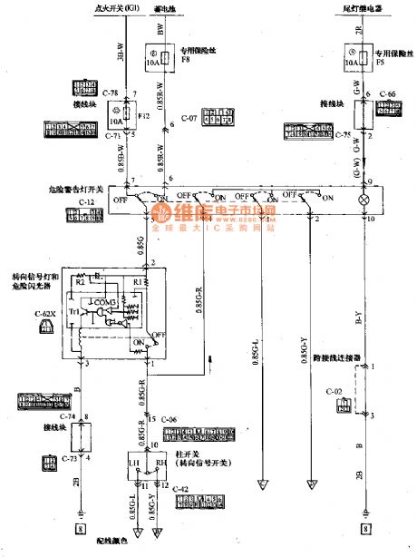
Mitsubishi Pagerlo light off-road vehicle directional signal light and hazard warning light connection circuit diagram
Published:2011/4/27 2:44:00 Author:Nicole | Keyword: Mitsubishi Pagerlo, light off-road vehicle, directional signal light, hazard warning light
View full Circuit Diagram | Comments | Reading(1143)
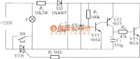
Floodlight power failure self-lock switch circuit
Published:2011/4/22 19:21:00 Author:Nicole | Keyword: floodlight, power failure, self-lock switch
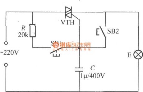
The floodlight is controlled by a ordinary stayguy switch, if it is power failure, it will be hard to differentiate whether the light is off, after it has power, the light will turn on all night, it is a waste of energy. If using this circuit to replace the ordinary stayguy switch, it will avoid this shortage, because it can beself-locked, the light will not be turned on. VTH should depend on the floodlight power, generally, it can use BCR3AM small plastic package TRIAC(3A/600V). (View)
View full Circuit Diagram | Comments | Reading(567)
Battery charge protection circuit composed of PTC component and overvoltage protection component
Published:2011/4/27 1:33:00 Author:Nicole | Keyword: Battery charge, PTC component, overvoltage protection component
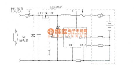
PTC component and overvoltage protection component work together to complete the following jobs: 1, Aiming at the large current which perhaps damage FET and batteries, it protects the current. 2, When it is reversed polarity, PTC action is used to limit the overcurrent produced by the zener diode positive conduction. 3, When the overvoltage component is protecting the voltage overload, the conduction current is limited by component. (View)
View full Circuit Diagram | Comments | Reading(1553)
Peak value hold circuit diagram composed of μPC151A
Published:2011/4/27 2:13:00 Author:Nicole | Keyword: peak value
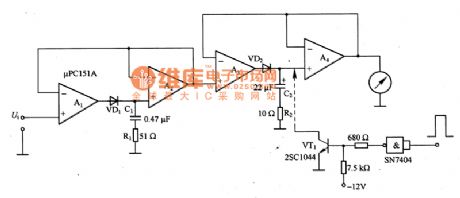
The figure of a peak value hold circuit composed of μPC151A is as shown. It is a peak value hold circuit and used to measure pulse. The first level peak value hold circuit is composed of A1 and A2, the capacity of charge capacitance should be as small as possible, then the peak value of inout singal will fast charge to it. The second level peak value hold circuit is composed of A3 and A4, charge capacitance C2 should use larger capacitance, then it can obtain the needed longer hold time. C2 should choose button capacitance.
(View)
View full Circuit Diagram | Comments | Reading(1790)
Ultrasonic remote control delay light receiver
Published:2011/4/25 4:34:00 Author:Nicole | Keyword: ultrasonic, remote control, delay light receiver
The figure is as shown, it is a delay light circuit uses ultrasonic as remote control command, when you use it, just to press the ultrasonic remote control transmitter(as below), the light will light up. Delaying about 1 min, the light will off automatically, it is very suitable for the use of getting up temporarily at night.
B1、B2 adopt well-assorted UCM-T40 and UCM-R40 piezoelectric ceramics ultrasonic transmit-receive converter.
(View)
View full Circuit Diagram | Comments | Reading(1016)
SH-818 high quality dual - tone seven functions color lamp control circuit
Published:2011/4/26 4:16:00 Author:Nicole | Keyword: color lamp
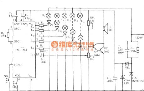
The circuit is as shown. SH-818 is made as the coretoformthis circuit. SH-818 is a high quality disyllable seven functions color lamp control circuit, it has many kinds of flashing patterns change programs, and with multiple double piano musics, the color lamp patterns will be changed with the music rhythm, then it will produce wonderful visual and audio effects. (View)
View full Circuit Diagram | Comments | Reading(536)
l MHZ LED pulse modulation circuit
Published:2011/4/26 22:48:00 Author:Nicole | Keyword: LED, pulse modulation
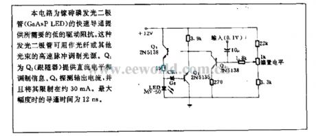
This circuit provides GaAsP LED's fast conduction with low drive resistance. This LED can be used as optical fiber or other beam high speed pulse modulation source. Q1 provides Q3(follower)with DC level and modulation information. Q2 detects output current, and it limits the current within 30mA. The conduction time is 12ns when it is maximum range. (View)
View full Circuit Diagram | Comments | Reading(810)
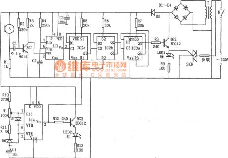
Double SCR stepless voltage regulation circuit
Published:2011/4/26 22:13:00 Author:Nicole | Keyword: Double SCR, stepless voltage regulation
View full Circuit Diagram | Comments | Reading(922)
TWH9104 festival color lamp with laughter control circuit
Published:2011/4/22 19:51:00 Author:Nicole | Keyword: festival color lamp, laughter
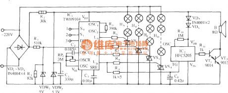
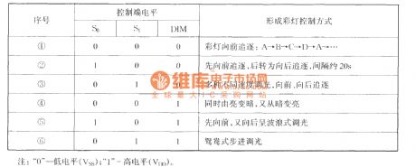
Relation between color lamp and control level is as below:
(View)
View full Circuit Diagram | Comments | Reading(503)
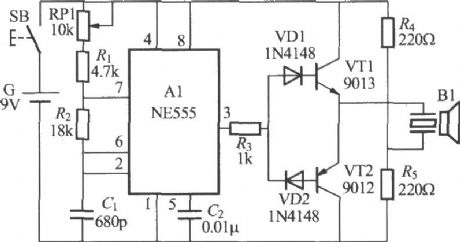
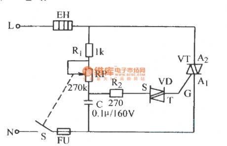
Delay light circuit with TRIAC(1)
Published:2011/4/26 4:26:00 Author:Nicole | Keyword: Delay light, TRIAC
The circuit is as shown, it is a delay light circuit adopts TRIAC. In addition to C1、C2、R4, the delay time is also related to the time of press key. VTH adopts MAC94A4、MAC97A6 TRIAC, the β value of VT1、VT2 should be more than 200. (View)
View full Circuit Diagram | Comments | Reading(2893)
SCR AC switch
Published:2011/4/22 18:57:00 Author:Nicole | Keyword: SCR, switch
Although bidirectional SCR is suitable for AC load switch, it should adopt unidirectional SCR when the work voltage is high or the load current is large. In figure, the circuit SCR gate is controlled by small transformer output rectified voltage loop directly. The advantage of using DC trigger is: it can connect high resistance load circuit.
Technical data of this circuit: work voltage: 380V; load resistance: 500Ω~80kΩ; control current: about 6.5mA.
Transformer data: the number of windings n1: 7400 turns, 0.08mm enameled copper wire; the number of windings n2, n3: 230 turns, 0.25mm enameled copper wire. (View)
View full Circuit Diagram | Comments | Reading(752)
High speed TTL probe circuit
Published:2011/4/17 8:00:00 Author:Nicole | Keyword: TTL probe
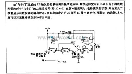
RS trigger is connected by NAND gate , it can test very narrow pulse, the narrowest pulse width is equal to the total delay time(about 30ns) of trigger's two NAND gate . When it appears pulse, the circuit will change the state, and it displays the output state of tigger by LED. After finding out the pulse, it must use K2 to reset the circuit. According to the choice of K1, this circuit will be in response to the positive pulse or negative pulse. (View)
View full Circuit Diagram | Comments | Reading(579)
SN75365 Four TTL-MOS Driver Circuit
Published:2011/4/26 9:00:00 Author:TaoXi | Keyword: Four, TTL-MOS Driver
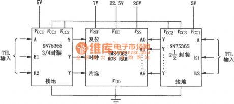
The SN75365 is one kind of TTL-MOS driver that has four NAND functions, this device is the connector between TTL circuits and high current or high voltage systems, so it drives the large capacitive loads andcan be usedwith a variety of common-MOS or RAM device. Also this device has the high-conversion speed, low power consumption, and each two drives have two public enable input pins, and the SN75365 has standard bipolar and MOS-circuit power supply. The wiring diagram of the SN75365 of type 4062 P-channel MOS RAMis as shown.
(View)
View full Circuit Diagram | Comments | Reading(1441)
The Circuit Of Multi-Channel Demodulator Of CD4051 and CH3130
Published:2011/4/26 8:57:00 Author:TaoXi | Keyword: Multi-Channel Demodulator
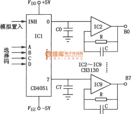
This circuit is composed of the (View)
View full Circuit Diagram | Comments | Reading(2518)
Anti-interfere voice control switch circuit
Published:2011/4/26 20:14:00 Author:TaoXi | Keyword: Anti-interfere, voice control switch
The anti-interfere voice control switch circuit is as shown:
(View)
View full Circuit Diagram | Comments | Reading(1034)
TC909OBN9 digital hang-shaped filter-type Y/C separation circuit
Published:2011/4/26 8:54:00 Author:TaoXi | Keyword: digital hang-shaped, filter-type Y/C separation
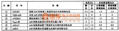
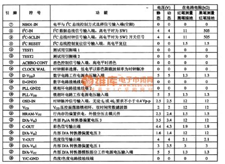
The TC909OBN9 is designed as one kind of digital hang-shaped filter-type Y/C separation circuit which is produced by the TOSHIBA company, and this device can be used in new large-screen color TV sets.
1.Features
The TC909OBN9 is composed of the video A/D converter, the D/A converter, the I2C bus interface circuit, the PLL VCO circuit and the Y/C separation circuit.
2.Pin functions and data
The TC9090BN is in 28-pin dual in-line package, the pin functions and data is as shown in table 1.
Tip: If the digital Y/C circuit failure, please check the RC components outside the TC909OBN(20)-pin.
Table 1. The pin functions and data of the TC9090BN (View)
View full Circuit Diagram | Comments | Reading(462)
Konka 60P Movement Rear Projection TV Failure Protection Circuit
Published:2011/4/26 18:38:00 Author:Christina | Keyword: Movement Rear Projection TV, Konka 60P, Failure Protection
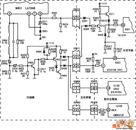
The Konka 60P Movement Rear Projection TV Failure Protection Circuit is as shown:
(View)
View full Circuit Diagram | Comments | Reading(614)
High speed Rise-edge triggered switch circuit composed of MIC5158
Published:2011/4/26 20:08:00 Author:TaoXi | Keyword: High speed, Rise-edge triggered switch
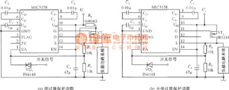
The high speed Rise-edge triggered switch circuit is as shown:
(View)
View full Circuit Diagram | Comments | Reading(514)
| Pages:280/312 At 20261262263264265266267268269270271272273274275276277278279280Under 20 |
Circuit Categories
power supply circuit
Amplifier Circuit
Basic Circuit
LED and Light Circuit
Sensor Circuit
Signal Processing
Electrical Equipment Circuit
Control Circuit
Remote Control Circuit
A/D-D/A Converter Circuit
Audio Circuit
Measuring and Test Circuit
Communication Circuit
Computer-Related Circuit
555 Circuit
Automotive Circuit
Repairing Circuit