
Control Circuit
Index 64
Language circuit controlled by phototransistor
Published:2012/8/19 22:50:00 Author:Ecco | Keyword: Language circuit , phototransistor
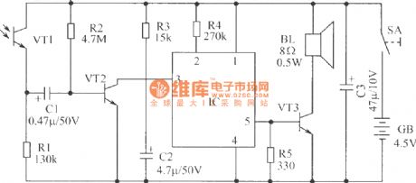
It consists of the light control switch and 35 voice IC. In the figure, photosensitive transistor VT1 and crystal transistor VT2, resistors R1 , R2, R3 and capacitors C1 , C2 , etc. constitute the light control switch circuit. Voice integrated circuit IC, transistor VT3 and resistors R4, R5 , etc. constitute a voice amplification circuit. Under the usual light source, VT1 showes a low resistance state, VT2 is in saturated conduction state, IC trigger side-pin 3 does not work without positive trigger pulse, then speaker keeps silent. When VT1 is obscured by the object, it will generate a negative pulse voltage which is coupled to VT2 base through C1, leading to VT2 into the cut-off state, then IC gets a positive trigger pulse to work, and the output audio signal is amplified through VT3 to promote the speaker emit sound.
(View)
View full Circuit Diagram | Comments | Reading(1167)
Burglar alarm circuit composed of photodiode
Published:2012/8/19 22:36:00 Author:Ecco | Keyword: Burglar alarm , photodiode
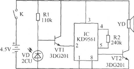
The alarm is mounted in a drawer. If the thief opens your drawer at night, the alarm will send the souud of ow - ow to warn thieves, and they will dare to start. Photosensitive diode VD, transistor VT1 and resistor R1 form a light control switch; integrated circuit IC, transistor VT2 and speaker YD form the alarm circuit. IC uses the KD-9561 four-tone analog alarm audio Manifold. VT1 and VT2 select 3DG201 silicon transistor with β value being greater than 60. VD selects 2CU photodiode. R1 and R2 use 1W carbon film resistors. YD uses 2.5 inches of electric speaker with impedance in 8Ω. Power select 3 and 5 battery. K selects small, self-resetting and normally closed contact button switch.
(View)
View full Circuit Diagram | Comments | Reading(2590)
Light-operated potentiometer circuit composed of phototransistor
Published:2012/8/19 22:58:00 Author:Ecco | Keyword: Light-operated, potentiometer , phototransistor
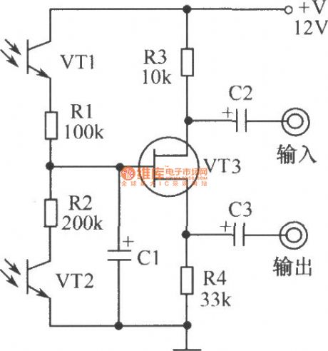
Light-operated potentiometer shown as the figure uses the laser pointer for light source to reflect light to photodiode VT1, then the channel resistance reduces, the volume increases; if the irradiation on VT2 reduces, the volume declines, therefore to achieve light-operated volume adjust. Every time you turning on the potentiometer, the VT3 tube's G potential is 0V, the channel resistance is in the maximum value, the volume will be kept the minimum value. The figure shows a mono, if you need to control multiple channels, you only need to connect FET G pole in parallel. The VT3 selects 3DJ6F or similar FET. VT1, VT2 is available to use commercial NPN photodiodes, C1, , C2 , C3 use 6.3μF/25V tantalum electrolytic capacitors. Resistor selects 1/8W metal film resistor.
(View)
View full Circuit Diagram | Comments | Reading(1662)
Seal machine control circuit
Published:2012/8/19 22:31:00 Author:Ecco | Keyword: Seal machine , control
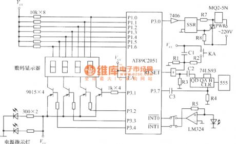
(1) It can prevent the program into an infinite loop. In order to improve the system's interference to prevent the program to enter an infinite loop, the system uses the WATCHDOG circuit composed of the counter. 555 is connected as multivibrator with cycle in t0; 74LS93 is connected as hexadecimal counter, when it counts to 8th pulse, QD side becomes high, microcontroller uses P3.7 output to clear pulse. If the cleared pulse interval is shorter than the eight pulse cycle, the counter will never be less than 8, and the QD side keeps low. When CPU receives interference and falls into infinite loop, it can not send reset pulse, the counter will soon count to 8, then QD side goes high immediately, but differential circuit C2 , R3 can output a positive pulse to make CPU is reset.
(View)
View full Circuit Diagram | Comments | Reading(1389)
Thermostat schematic of thermistor electric water heater
Published:2012/8/16 22:27:00 Author:Ecco | Keyword: Thermostat schematic , thermistor, electric water heater
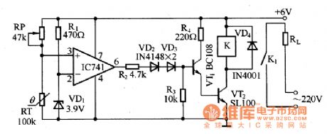
The circuit consistes of thermistor RT, comparator, driverand heater RL. The circuit can keep water temperature at 90 ℃ by automatically opening and closing control of the heater.
When temperature is at 25 ℃ thermistor resistance is 1OOkΩ, temperature coefficient of 1K / ℃. When comparator's inverting input end is added the 3.9V reference voltage, the comparator's noninverting input terminal is added the partial pressure voltage of RP and thermistor RT. When the water temperature belows 90 ℃, the comparator IC outputs high potential to drive VT1 and VT2 conduction, then the relay K works, heater circuit is closed; when the temperature is higher than 90 ℃, comparator IC output is in low potential, VT1 and VT2 are cut-off, the heater circuit is disconnected by relay K. Adjusting RP obtain the required water temperature.
(View)
View full Circuit Diagram | Comments | Reading(4234)
Infrared burglar alarm circuit schematic
Published:2012/8/16 21:10:00 Author:Ecco | Keyword: Infrared , burglar alarm
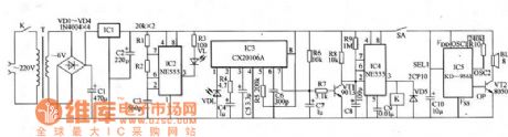
Infrared burglar alarm circuit schematic is shown in Figure 1. Infrared transmitter is a multivibrator with oscillation frequency being 40kHz, and it is composed of IC2 ( NE555 ), R1 , R2 and C3. VLS is the infrared emission probe which can be used to radiate 40kHz high-frequency externally to form the IR beam. VDL is the infrared receiver probe, and it forms infrared receiver, shaping and amplifying circuit with IC3 (CX20106A), and the infrared signal can be converted into electrical pulses after being amplified. IC4 and its peripheral components form alarm implementation circuit, once pin 2 is in low level, the circuit immediately flips, then the signal output end pin 3 is immediately converted to high level output, and it has delay function at the same time. Usually , VDL receives the infrared beam being radiating by VDL.
(View)
View full Circuit Diagram | Comments | Reading(2401)
Y-connection motor protection circuit
Published:2012/8/11 1:35:00 Author:Ecco | Keyword: Y-connection , motor , protection
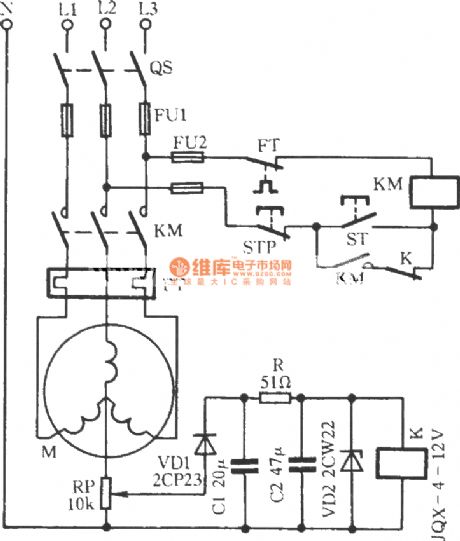
In the circuit shown as the figure, pressing the ST will make KM coil get electric and pull in; loosening ST will allow the KM to get self-protection, then motor M runs. When one phase of three-phase alternating current circuit is dieconnected, then motor's midpoint will generate potential difference. The voltage will be rectified and stabilized to make relay K be energized, then the power of M is cut to to protect the motor stator windings from burning. The circuit is suitable for motors with power lowering than 7.5kW.
(View)
View full Circuit Diagram | Comments | Reading(2065)
The water height alarm circuit diagram
Published:2012/8/6 4:23:00 Author:Ecco | Keyword: water height , alarm
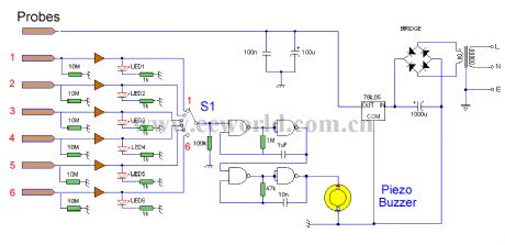
This circuit will trigger with any fluid with a resistance under 900K between the maximum separation distance of the probes. Let me explain further. The circuit uses a 4050B CMOS hex buffer working on a 5 volt supply. All gates are biased off by the 10M resistors connected between ground and buffer input. The common probe the topmost probe above probe 1 in the diagram above is connected to the positive 5 volt supply. If probe 1 is spaced 1 cm away from the common probe and tap water at 25 ?C is detected between the probes (a resistance of 20k) then the top gate is activated and the LED 1 will light. Similarly if probe 2 at 2 cm distance from the common probe detects water, LED 2 will light and so on. Switch 1 is used to select which output from the hex buffer will trigger the audible oscillator made from the gates of a CMOS 4011B IC.Placement of Probes:As 7 wires are needed for the probe I reccommend the use of 8 way computer ribbon cable. The first two wires may be doubled and act as the common probe wire. Each subsequent wire may be cut to required length, if required a couple of millimetres of insulation may be stripped back, though the open cut off wire end should be sufficient to act as the probe. The fluid and distance between probe 6 and the common probe wire must be less than 900k. This is because any voltage below 0.5 Volt is detected by the CMOS IC as logic 0. A quick potential check using a 900k resistance and the divider formed with the 10M resistor at the input proves this point: 5 x (0.9 / (0.9+10) = 0.41 Volt. (View)
View full Circuit Diagram | Comments | Reading(1842)
Neon patterns controlling circuit ( DNL9100 )
Published:2012/8/1 2:37:00 Author:Ecco | Keyword: Neon patterns , controlling circuit
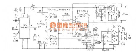
The circuit is shown as the figure. It includes the oscillation pulse signal source, octal counting / pulse divider, AC solid state relay driver circuit, neon high-voltage transformerand power supply, etc. .
(View)
View full Circuit Diagram | Comments | Reading(1156)
2D lamp controller
Published:2012/7/25 2:59:00 Author:Ecco | Keyword: 2D lamp , controller
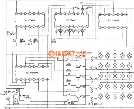
As shown in the figure, the circuit is mainly composed of the NAND gate IC1 (CD4096), counting / timing distribution circuit IC2 (CD4017), analog electronic switch IC3 (CD4066) and D trigger IC4 (CD40174). The lamp controller can control five groups of Lanterns to be lit and extinguished progressively. If a certain number of lanterns are connected in combination, you can create a scene with color change on the plane. It is more rich and colorful than usually control the flowing of the color in a line.
(View)
View full Circuit Diagram | Comments | Reading(2341)
AD603 voltage gain control circuit
Published:2012/7/23 2:42:00 Author:Ecco | Keyword: voltage gain control
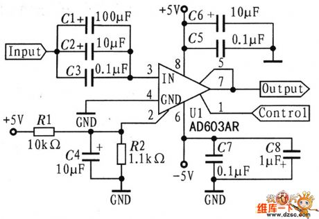
This circuit uses two AD603 cascades to realize controllable gain range in 0 dB ~ 60 dB. AD603 monolithic gain range is 10 dB ~ 30 dB, and the range of input control voltage is 0 V ~ l V. Among them, the first-stage AD603 circuit diagram is shown as the figure. As AD603 input impedance is 100 Ω, it must add input buffer to improve the input impedance, then to meet the requirements of the system resistance. In addition, as the front-end circuit affects the noise of the circuit, the circuit uses the amplifier circuit composed of primary op amp AD620 as a pre- amplifier to reduce the noise.
(View)
View full Circuit Diagram | Comments | Reading(3115)
The protection circuit composed of negative resistance LED
Published:2012/7/18 2:50:00 Author:Ecco | Keyword: protection circuit , negative resistance, LED

View full Circuit Diagram | Comments | Reading(963)
MCU control circuit diagram
Published:2012/7/16 2:52:00 Author:Ecco | Keyword: MCU control
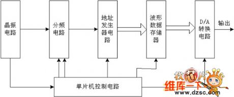
The design of arbitrary waveform generator uses MATLAB's powerful simulation functions, and it can provide the frequency, cycle, pulse width of arbitrary waveform data conveniently and fastly; and data is stored in data memory. Under the control of the microcontroller, it uses CPLD circuit to generate and read the address. then the data is sent into the D / A converter circuit to get arbitrary waveform signal. The system block diagram is shown in Figure 1; The frequency dividing circuit and address generator is realized by the CPLD.
(View)
View full Circuit Diagram | Comments | Reading(1127)
60h timing circuit
Published:2011/12/1 21:39:00 Author:May | Keyword: 60h timing
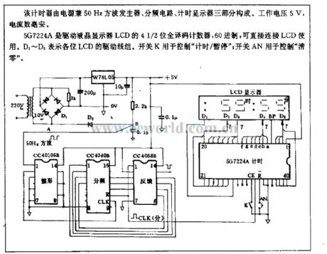
This timer consists of three parts: power supply double 50Hz square wave generator, frequency dividing circuit, timing display. Its working volt is 5V. Its current is several milliampere.
5G7224A is 4 1/2 bit fully decoded counter driving LCD. It is 60 system and it can direct-coupling LCD. D1~D5 state each bit LCD drive line group. Switch K is used for controlling time/suspend ; Switch AN is used for controlling zero clearing .
(View)
View full Circuit Diagram | Comments | Reading(1837)
Light gradually, gradually eliminate type lamp dimmer circuit
Published:2011/4/24 1:18:00 Author:May | Keyword: lamp dimmer
The diagram is lamp dimmer which has the function of light gradually, gradually eliminate. It does not appear the light stimulation of the human eye when the lights suddenly illuminated , and also can reduce the damage when open lamp impact current to the bulb, circuit is shown in the diagram. This circuit is LED driver circuit in optocoupler which consists of a six inverter circuit, in order to add the driver ability of the circuit, four inverters are use in parallel.
(View)
View full Circuit Diagram | Comments | Reading(2153)
Gas - smoke alarm circuit with Triac
Published:2011/8/29 1:34:00 Author:Jessie | Keyword: Gas - smoke alarm , Triac
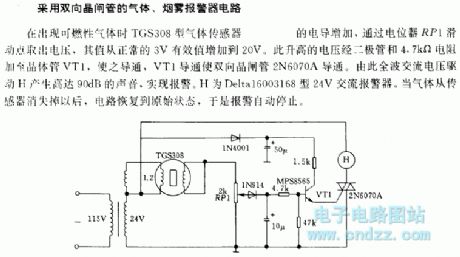
When it appears combustible gas, the conductanceof gas sensor TGS308will increase.The voltageon potentiometer RP1 sliding points increases from normal 3V to 20V. This increased voltage is added to the transistor VT1 and makes it turn on by the diode and 4.7Ω resistor, then the Triac 2N6070A is turned on. Full-wave AC voltage drives H to produce 90dB sound and alarm. H is 24V AC Delta16003168 alarm. When the gas disappears from the sensor, the circuit recovers to its original state, so the alarm automatically stops. (View)
View full Circuit Diagram | Comments | Reading(1777)
Safe and reliable delay switch circuit
Published:2011/8/29 2:04:00 Author:Jessie | Keyword: delay switch circuit
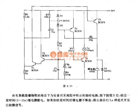
It should use the safe and reliable delay switch circuit shown as the chart in the places with flammable and explosive materials. After pressing button S anda certain time, therelay is cut off. If in a given time, therelay doesn't release, so indicator La isextinguished and sent out the fault signal.
Technical parameters: Working voltage: 24V; delay time(adjusted by R4): 3~15s. (View)
View full Circuit Diagram | Comments | Reading(1469)
Delay switch circuit with thyristor
Published:2011/8/29 2:01:00 Author:Jessie | Keyword: delay switch circuit
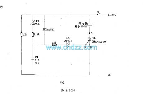
Delay switch circuit with thyristorcan control the connect and disconnect of high-power appliances. The delaying accuracy of the Figure (a) depends on regulator. Figure (b) uses two-way diode A9903 or TV503 to replace the tetrode BRY20 in Figure (a). Technical parameters: 60V ± 10%; maximum load resistor RL: 860Ω, the minimum load resistor RL: 100Ω, delay time: 0.3 ~ 3.6S.
(View)
View full Circuit Diagram | Comments | Reading(2038)
Common transistor electronic relay for controlling base
Published:2011/8/29 1:54:00 Author:Jessie | Keyword: controlling base , transistor electronic relay
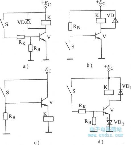
Figure A is the NPN transistor using + Ec electronic power control relay. Figure b is grounded NPN transistor control circuit. Figure c is the PNP transistor with Ec-controlled electronic relay. Figure d is the self-bias electronic relay. (View)
View full Circuit Diagram | Comments | Reading(3598)
Touch delay light circuit with digital circuit(5)
Published:2011/7/28 2:07:00 Author:Nicole | Keyword: Touch delay light, digital circuit
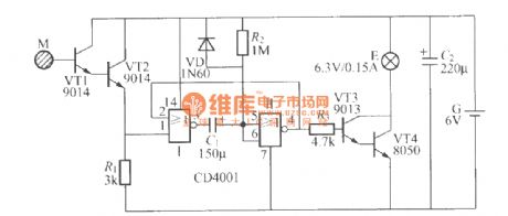
The figure is as shown, it is a touch delay light circuit which adopts dry battery as power supply, it can be put beside thepillow, at night, if you touch the sheet metal M of that small box, the small light E will keep lighting for about 2 minites automatically. (View)
View full Circuit Diagram | Comments | Reading(1171)
| Pages:64/312 At 206162636465666768697071727374757677787980Under 20 |
Circuit Categories
power supply circuit
Amplifier Circuit
Basic Circuit
LED and Light Circuit
Sensor Circuit
Signal Processing
Electrical Equipment Circuit
Control Circuit
Remote Control Circuit
A/D-D/A Converter Circuit
Audio Circuit
Measuring and Test Circuit
Communication Circuit
Computer-Related Circuit
555 Circuit
Automotive Circuit
Repairing Circuit