
Control Circuit
Index 81
Solid-state relay circuit diagram exchanged and controlled by the microcomputer control
Published:2011/8/18 2:10:00 Author:Jessie | Keyword: Solid-state relay, microcomputer
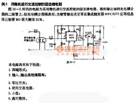
This circuit is a Solid-state relay circuit diagram exchanged and controlled by the microcomputer control. Computer output is added to the photoelectric coupler diode,then it isisolated by electricity couplers, after photosensitive pipe output, it issent to zerovoltage integrated flip-flop MFC8070, amplifier SCR by transistor BG. Circuit performances: four sections of form; Input/output high insulation isolation; Zerovoltage switch; Use theAC power; Small; High reliability. (View)
View full Circuit Diagram | Comments | Reading(1251)
Positive and negative half cycle two SCR trigger principle circuit
Published:2011/8/18 2:11:00 Author:Jessie | Keyword: Positive and negative half cycle, SCR trigger
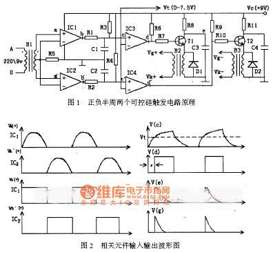
The circuit is composed bya synchronous transformerB1, two pulse transformersB2, B3, two Dual voltage comparators LM393 (or a four voltage comparator LM339) and two transistors (T1 and T2). (View)
View full Circuit Diagram | Comments | Reading(2052)
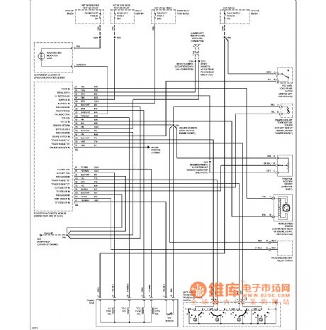
Buick transmission circuit diagram(3.8l,vink)
Published:2011/8/18 0:50:00 Author:Jessie | Keyword: Buick transmission , 3.8l,vink
View full Circuit Diagram | Comments | Reading(918)
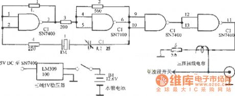
1MHz crystal calibrator circuit diagram
Published:2011/8/18 0:51:00 Author:Jessie | Keyword: 1MHz crystal calibrator
View full Circuit Diagram | Comments | Reading(1384)
Panasonic GD90 mobile physical maintenance circuit diagram
Published:2011/8/17 21:50:00 Author:Jessie | Keyword: mobile physical maintenance
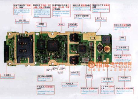
View full Circuit Diagram | Comments | Reading(1376)
Visual doorbell circuit 1
Published:2011/8/17 21:19:00 Author:Jessie | Keyword: Visual doorbell
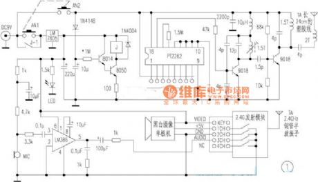
Thefigureshows the outdoor circuit, andAN1, AN2are the bell buttons, when a guest visits to press a button switch, the power all the wayprovides powerforcoding launch circuit through the AN2, and it transmits 315MHz coding signal, and the 1N4148charges to 10 uF timing capacitor. Theother way can providepower suppliesfor delay circuitby AN1, then relaygets power and is connected, thenits contact J-1 isclosedfor self-protection. Meanwhile LM386composes voice test circuit, cameras and 2.4 GHztransmitting modulewill get powertowork, thentrasmitting module emits a high frequency signal that modulated by AV.
(View)
View full Circuit Diagram | Comments | Reading(844)
Visual doorbell circuit 2
Published:2011/8/17 21:30:00 Author:Jessie | Keyword: Visual doorbell
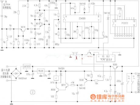
Figure shows the 315MHz code receiving signal demodulation and controlling circuit. 315MHz code signal is sent to CD4069 for shanping and amplification after high amplification and superregeneration demodulation, then the PT2272 decoding outputs a high level to trigger the music IC to issue the ding-dong, ding-dong doorbell. Meanwhile, the ring signal can turn on the control circuit, then relay J makes action, and the total powerof TV works. The control circuit also has a delay circuit, and after about 55 seconds, the relay releases, the total power of TV is turned off, then it will be in the re-standby state. Note: the address code of the PT2272 decoding block must be the same with encoding block PT2262. (View)
View full Circuit Diagram | Comments | Reading(1564)
Visual doorbell circuit 3
Published:2011/8/17 21:43:00 Author:Jessie | Keyword: Visual doorbell
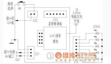
This is 2.4 GHz baseband demodulation plate. Plate directional antenna receives 2.4 GHz signal and sends it to 2.4 GHz receiving module toisolateaudio and video signals, then the baseband clutter signal is filtered out by subsequent circuit, then it ismagnified into standard AV signal output, then it is input to TV. The 2.4 GHz transceiver module, 2.4 GHz transceiver antenna, 2.4 GHz baseband demodulation board and black and white veneer camera in thesystem are all from shenzhenYoujin electronic Co., LTD.
Hollow inductor uses ∮ 1.0mm enamelled wire to wound in ∮ 5mm wire rod with the turns which is marked in the figure. (View)
View full Circuit Diagram | Comments | Reading(769)
A special kind of power circuit
Published:2011/8/17 21:37:00 Author:Jessie | Keyword: power circuit
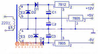
Although this circuit's structure is simple, it can produce three groupsof dc voltage fromtwo same secondary windings, andthey are + 5V, - 5V and + 12 v that certain microprocessors need. The characteristic of circuit is the connection way of D2 and D3, and they areconnected between E2, E3, andthese two groups ofAC power play a role of whole wave rectifier. In the positive half cycle, E2 charges for C2 through D2 , and current travelling b→C2(+)→C2(-)→D2→a; In a negative half cycle, E3 charges forC3through D3 , current travelling d→D3→C2(+)→C2(-)→C. Diodes D1 and D4are the general half wave rectifiers. (View)
View full Circuit Diagram | Comments | Reading(710)
Human body induction switch circuit diagram
Published:2011/8/17 21:03:00 Author:Jessie | Keyword: human body , induction switch
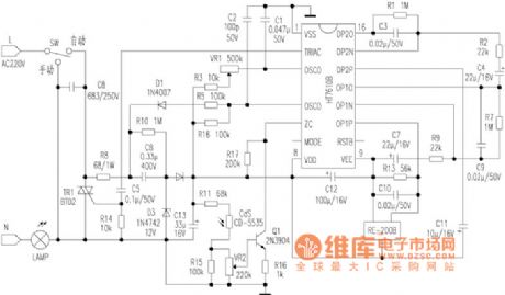
When the switchSWis on the automatic position, RE - 200B will attune the infrared that human releaseand convert it to faint signals sent to HT7610B's pin 11.With internal level 2 amplifier and resistance, pin 20 outputs 0.3 ~ 3 HzAC signal, when this signal's amplitude is over 2V,pin 2will output a square-wave voltage that synchronous with AC power voltage todrive bidirectional triode thyristorfor zero trigger conduction, then the light is turned on.
VR1 is the delay time adjustment potentiometer, afetr lamp beinglit, lights turning off time delay can be adjusted between8-6 seconds; VR2is the light and dark adjusting potentiometer.
(View)
View full Circuit Diagram | Comments | Reading(2046)
Simple gas and fog alarm circuit
Published:2011/8/17 21:10:00 Author:Jessie | Keyword: gas and fog alarm
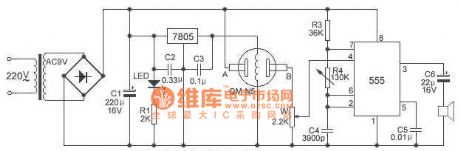
555 time-based circuitforms theself-excited monostable multivibrator, and itusesingeniouslyreset server to trigger. When gas-sensitive device access to flammable gas, its resistance reduces, thenthe time-based circuit's reset end potential rises. When integrate block is in1/3 working voltage, it willsend outa warning signal, so it has the characteristics of high sensitivity.
Power transformer B's output poweris greater than 5W, and the secondary voltageis 9V. Gas sensor uses QM-N5 or MQ211, which is a relatively strong universal gas sensor for natural gas, coal gas, liquefied petroleum gas, gasoline, carbon monoxide, hydrogen, alkanes and so on.
(View)
View full Circuit Diagram | Comments | Reading(812)
Combustible gas alarm circuit diagram
Published:2011/8/17 21:14:00 Author:Jessie | Keyword: Combustible gas, alarm
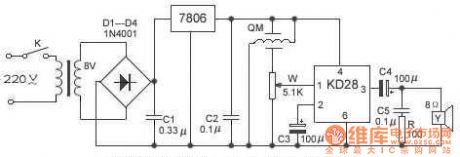
We usethe KD28 gas sensor probeand several componentstomake a combustible gas alarm device. When the combudstible gas of surrounding environment exceed a certain concentration, it can remind peopleto takemeasures.
Debugging: adjusting W (1 minute later) can make circuit not alarm, and thenwe access gas lighters (butane) to gas-sensitive element alarm untilitreturns normal work after gas left. This device's features are less component, commissioning simple. Itcan be usedin the detection of flammable gas such as gas, liquefied petroleum gas, natural gas and smoke etc.
(View)
View full Circuit Diagram | Comments | Reading(876)
One-touch switch circuit diagram
Published:2011/8/17 20:24:00 Author:Jessie | Keyword: One-touch switch
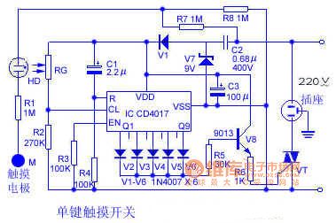
The circuit diagram is as shown, HD is atubular neon bulb, photoconductive resistance RG and it composes of homemade photoelectric couplers , and forms touch signal input pathwaywith touch electrodes M, R1. CD4017's Q1, Q3, Q5, Q7, Q9 odd output terminalconnects diode V2 ~ V6 respectively, when one of them output high electricity, V8 is connected and trigger bi-directional thyristor VT to connect, load accesses to socket and works,while Q2, Q4 even output terminal impending; Conversely, whenthe even output oneis high electricity, V8, VT are all disconnected, socket load disconnects, when the touch switch just connects,since C1, R4's differential effect, CD4017 automatic reset, socketis de-energized.
(View)
View full Circuit Diagram | Comments | Reading(2166)
The semiconductor SCR AC regulator circuit
Published:2011/8/23 22:06:00 Author:Borg | Keyword: semiconductor, SCR, AC regulator
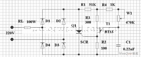
SCR is a kind of new semiconductor, which characterizes small size, low weight, high efficiency, long lifespan, fast action and convenient usage,etc, by far, AC regulators are often SCR regulators. Here is to introduce a SCR AC regulator whose wiring is simple, installation is easy and control is convenient, which can be used as the domestic apparatus regulating equipment, it can regulate the light for the lighting lamp, regulate the speed for fans, regulate the temperature for irons and others. The output power of this regulator is 100W.
(View)
View full Circuit Diagram | Comments | Reading(2734)
The darkroom exposure meter circuit
Published:2011/8/23 22:06:00 Author:Borg | Keyword: darkroom, exposure meter
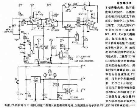
This exposure meter can not only measure the exposure time, but also indicate the difference in the relative photometry. In the circuit, D1 is the photoelectric diode, when it is shone by the light, it is generating a voltage which is amplified and phase-inverted by the 3-stage op-amps IC2, IC3 and IC4, the voltage is added on the serial circuit composed of the meter head M1, R18 and trimmer resistor P3, the application of the M1 dial is logarithm type. The diodes D2 and D3 are used to compensate the temperature voltage changes caused by the photoelectric tube, so it should be closed to D1 when we fix it.
(View)
View full Circuit Diagram | Comments | Reading(1530)
The light-test circuit with functions of power supply maintenance and auto cutoff
Published:2011/8/23 22:06:00 Author:Borg | Keyword: light-test circuit, power supply maintenance, auto cutoff
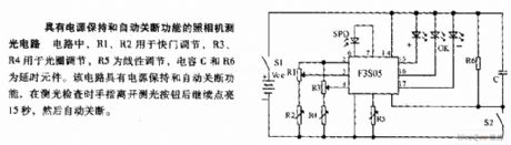
In the circuit, both R1 and R2 are used in shutter adjustment, both R3 and R4 are used in halo adjustment, R5 is the linearity adjuster, capacitor C and R6 are the time delay element. The circuit has the functions of power supply maintenance and auto cutoff, which can keep lighting for 15s after the finger leaves the key while light testing, and then turns off automatically.
(View)
View full Circuit Diagram | Comments | Reading(767)
The flashlight with auto dimming function circuit
Published:2011/8/23 22:06:00 Author:Borg | Keyword: flashlight, auto dimming function
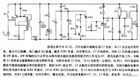
When the power supply switch K1 is put through, the step-up circuit is charging capacitor C7, when C7 is full, the Ne light is glowing, which means the shoot can be done. The shutter contactor K2 is on, which triggers SCR3 conducting, the flash tube is flashing, C7 is starting to discharge. At the same time, C1 is discharging reversely through stabilizer DW, the backward breakdown voltage drop on the 2 poles of DW provides for the light test trigger circuit with a 6V working voltage, the light test circuit is starting to work. (View)
View full Circuit Diagram | Comments | Reading(812)
The camera affiliated flash device circuit
Published:2011/8/23 22:07:00 Author:Borg | Keyword: flash device, camera
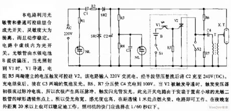
In the circuit, the light sensitive tube and ordinary SCR compose the light switch, the sensibility is increased, and the action is stable. In the dotted line frame is the light switch. The light sensitive tube bias voltage is provided by the mercury battery B, when the light is shed on V1, V1 is conducting, the voltage on the 2 terminals of resistor R5 triggers SCR V2. The circuit is input with 220V AC which charges C2 to 240V(DC) after being half-wave doubled and rectified. (View)
View full Circuit Diagram | Comments | Reading(790)
The camera flashlight circuit
Published:2011/8/23 22:07:00 Author:Borg | Keyword: camera flashlight
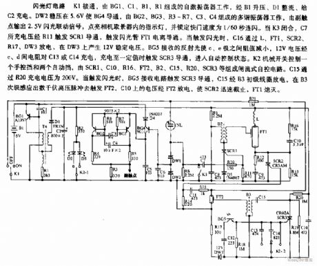
The camera flashlight circuit when K1 is put through, the self-motivation oscillator composing of BG1, C1, B1 and R1 is starting to work, after being boosted by B1 and rectified by D1, it is charging C2. DW2 makes BG4 conduct when it is 5.6v, the multi-resonance oscillator composed of BG2, BG3, R3~R7, C3 and C4 is getting into working, the 2.5V flash signal is output by the vice contactor, then the indicator in the camera viewfinder is glowing, and the shutter is locked and the 1/60 flash is continuous done. When K3 is pulled in, C7-charged voltage is triggered by R11 and SCR1 is conducting, the flash tube FT1 is also triggered and conducting.
(View)
View full Circuit Diagram | Comments | Reading(2441)
The Sound and light double control eight-channel color light 12 songs sound circuit (BH-SH-II)
Published:2011/8/30 2:24:00 Author:Christina | Keyword: Sound, light, double control, eight-channel, color light, 12 songs, sound circuit
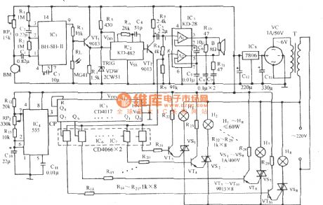
As the figure shows, it is composed of the voice-activated electronic switch, the light control switch, the music sound circuit, the audio power amplifier circuit, the multivibrator, the time order distribution circuit, the audio control switch circuit, the SCR drive circuit and the AC step-down rectifier circuit. When the circuit is playing the world famous songs, the eight-channel color light will send out the synchronous flash light.
(View)
View full Circuit Diagram | Comments | Reading(838)
| Pages:81/312 At 2081828384858687888990919293949596979899100Under 20 |
Circuit Categories
power supply circuit
Amplifier Circuit
Basic Circuit
LED and Light Circuit
Sensor Circuit
Signal Processing
Electrical Equipment Circuit
Control Circuit
Remote Control Circuit
A/D-D/A Converter Circuit
Audio Circuit
Measuring and Test Circuit
Communication Circuit
Computer-Related Circuit
555 Circuit
Automotive Circuit
Repairing Circuit