
Control Circuit
Index 100
SIGNAL_CONTROLLED_SWITCH
Published:2009/7/14 1:04:00 Author:May
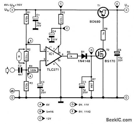
This signal-controlled switch actuates or deactuates AF equipment, including preamplifiers, power amplifiers, and filters. It is particularly useful for battery-operated equipment because, owing to the low current drain of 12 to 14μA, there is no need to switch the AF equipment off. When the switch has not detected any AF signal for 10 seconds, it switches off the supply to the equipment. (View)
View full Circuit Diagram | Comments | Reading(1214)
FULL_RANGE_CONTROL
Published:2009/7/14 1:02:00 Author:May
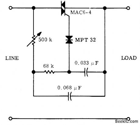
Triggered triac is used with double phase-shift network to obtain reliable triggering at conduction angles as low as 5°, as required for control of incandescent lamps and some motors. Triac rating determines size of load.- SCR Power Control Fundamentals, Motorola, Phoenix, AZ, 1971, AN-240, p 6. (View)
View full Circuit Diagram | Comments | Reading(1185)
SYNCHRONIZED_SWITCHING
Published:2009/7/14 1:02:00 Author:May
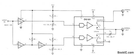
Transients occurring during switching between two amplifier channels are attenuated by synchronizing turn on of one switch in DG181 JFET analog switch with turnoff of other switch. Switching action is controlled by logic input,- Analog Switches and Their Applications, Siliconix, Santa Clara, CA, 1976, p 7-61. (View)
View full Circuit Diagram | Comments | Reading(826)
LOGIC_CONTROLLED_ANALOG_SWITCH
Published:2009/7/14 1:00:00 Author:May
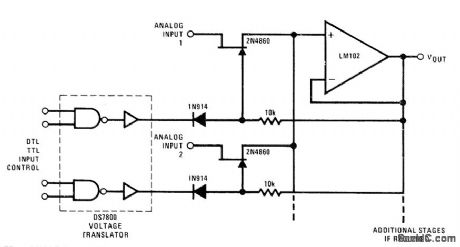
2N4860 JFETs were chosen for low leakage and 25-ohm ON resistance in switching circuit. LM102 opamp serves as voltage buffer. DS7800 IC provides switch drive under control of DTL or TTL levels.- FET Databook, National Semiconductor, Santa Clara, CA, 1977, p 6-26-6-36. (View)
View full Circuit Diagram | Comments | Reading(894)
DIAMOND_BRIDGE_ANALOG_SWITCH
Published:2009/7/14 0:55:00 Author:May
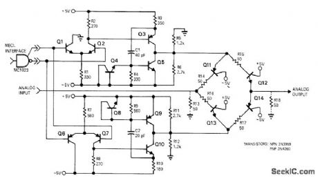
Analog signals up to 3 V P-P are switched in less than 3 ns to meet requirements of multiplexer and sample-and-hold portions of 100 Mb/s PCM telemetry encoder. Symmetrical drive circuits turn four-transistor diamond bridge on and off at 20-MHz clock frequency. Transient-coupled pullback transistors Q5 and Q9 speed turnoff. Typical rise time is 1,5 ns and fall time is 2 ns for 1-VDC analog input.-W. A. Vincent, Diamond Bridge Improves Analog Switching, EDN Magazine, Feb 15, 1971, p 41-42. (View)
View full Circuit Diagram | Comments | Reading(1611)
FET_ANALOG_SWITCH
Published:2009/7/14 0:51:00 Author:May
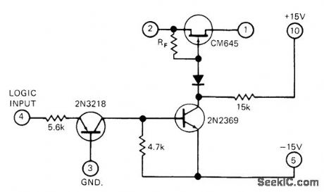
Simple level-shifting driver provides analog switching. Input of logic 1 makes emitter and collector current flow in input PNP transistor, for shifting from logic to -15 V. This current makes NPN transistor turn on so its collector is -15 V, diode is forward-biased, and FET gate is about -14.3 V. At logic 0, both transistors are off and driver output is at +15 V. Diode is now reverse-biased, turning FET on to provide desired switching action between outputs 1 and 2.-J. Cohen, Solid-State Signal Switching: Ifs Getting Better All the Time, EDN Magazine, Nov. 15, 1972, p 22-28. (View)
View full Circuit Diagram | Comments | Reading(2102)
FERRITE_CORE_SWITCHING
Published:2009/7/14 0:50:00 Author:May
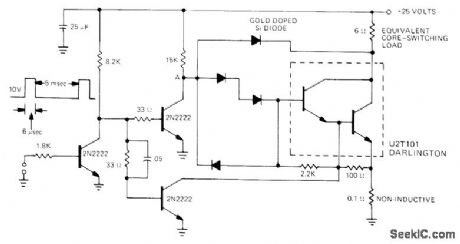
Darlington transistor driven by low-power current stage serves for saturating groups of ferrite cores in phased arrays for radar systems or in read/write core switching for memory systems. Circuit provides fast rise and fall times.- Designer's Guide to Power Darlingtons as Switching Devices, Unitrode, Watertown, MA, 1975, U-70, p 4. (View)
View full Circuit Diagram | Comments | Reading(977)
VIDEO_SWITCH
Published:2009/7/14 0:49:00 Author:May
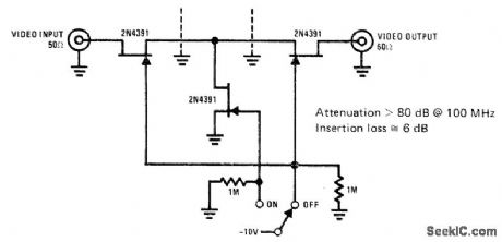
2N4391 FETs provide ON resistance of only 30 ohms and OFF impedance less than 0.2 pF, to give performance comparable to that of ideal high-frequency switch. Attenuation is greater than 80 dB at 100 MHz. Insertion loss is about 6 dB.- FET Databook, National Semiconductor, Santa Clara, CA, 1977, p 6-26-6-36. (View)
View full Circuit Diagram | Comments | Reading(0)
ANALOG_WITH_HIGH_TOGGLE_RATE
Published:2009/7/14 0:46:00 Author:May
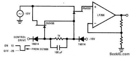
Simple commutator circuit provides low-impedance gate drive to PN4091 FET analog switch for both ON and OFF drive conditions. For high-frequency signal handling, circuit also approaches ideal gate drive conditions by providing low AC impedance for OFF drive and high AC impedance for ON drive.- FET Databook, National Semiconductor, Santa Clara, CA, 1977, p 6-26- 6-36. (View)
View full Circuit Diagram | Comments | Reading(823)
DIFFERENTIAL_ANALOG_SWITCH
Published:2009/7/14 0:45:00 Author:May
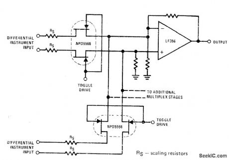
NPD5566 dual JFETs provide high accuracy for differential multiplexer because JFET sections track at better than ±1% over wide temperature range, close tracking reduces errors due to common-mode signals Values of resistors depend on application and on type of opamp used.- FET Databook, National Semiconductor, Santa Clara, CA, 1977, p 6-26-6-36. (View)
View full Circuit Diagram | Comments | Reading(0)
LIQUID_NITROGEN_LEVEL_CONTROL
Published:2009/7/14 0:35:00 Author:May
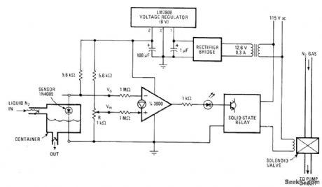
1N4005 diode serves as sensor. Junction voltage of diode increases from 0.7 V at room temperature to 1.05 V when in liquid nitrogen. Voltage change is used to activate amplifier that controls solenoid valve through solid-state relay.1K pot R adjusts circuit sensitivity; this can be set so pump starts refilling of container when liquid is as much as 2 inches below diode, to eliminate frequency recycling LED indicates valve status.-V.J.H. Chiu, Diode Sensor and Norton Amp Control Liquid-Nitrogen Level, Electronics, Feb.2,1978,p 117. (View)
View full Circuit Diagram | Comments | Reading(1146)
SΥNCHRONOUS_SWITCH
Published:2009/7/14 0:30:00 Author:May
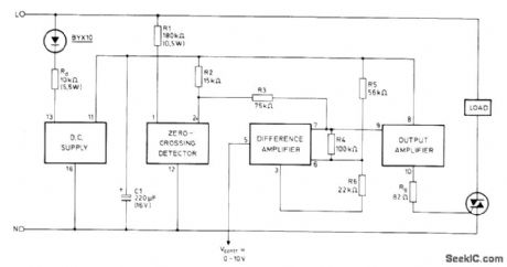
Mullard TCA280A trigger module provides triggering of load triac at zero crossings of AC line voltage. Values shown are for triac requiring gate current of 100mA; for other triacs, values of Rd, Rg, and C1 may need to be changed. Designed for resistive loads and ON/OFF rather than propoltional control.- TCA280A Trigger IC for Thyristors and Triacs, Mullard, London, 1975, Technical Note 19, TP1490, p 10. (View)
View full Circuit Diagram | Comments | Reading(1252)
FEEDBACK_CONTROL
Published:2009/7/14 0:22:00 Author:May
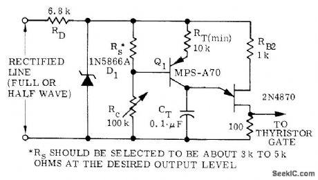
Replacement of manual phase control pot with sensor and transistor provides automatic control of load power in response to stimuli such as heat, light, pressure, or magnetic fields. Output of feedback control circuit goes to thyristor in series with load. RC establishes desired operating point for sensing resistor RS. As RS increases in resistance, more current flows into CT and makes 2N4870 UJT trigger at smaller phase angle so more power is applied to load. For opposite effect, interchange RS and RC.-D. A. Zinder, Unijunction Trigger Circuits for Gated Thyristors, Motorola, Phoenix, AZ, 1974, AN-413, p 4. (View)
View full Circuit Diagram | Comments | Reading(980)
SOUND_OPERATED_SWITCH
Published:2009/7/13 23:46:00 Author:May
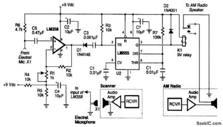
An electret microphone is placed directly in front of the scanner speaker. When the microphone (X1) picks up sound (usually voice) from the speaker, the sound signal is amplified and detected, activates a retriggerable one-shot circuit, and controls the relay (K1). The relay controls the AM radio speaker, muting it when sound is detected from the scanner. (View)
View full Circuit Diagram | Comments | Reading(0)
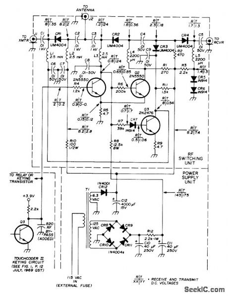
RF_SENSING_TB_SWITCH
Published:2009/7/13 23:43:00 Author:May
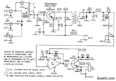
System detects presence of RF at output of transmitter and changes antenna connection from receiver to transmitter instantly and automatically. No modifications are required for transmitter or receiver. RF voltage divider R1 permits use with transmitters of any power. Broadband amplifier Q1 feeds voltage doubler CRl-CR2 through broadband toroidal step-down transformer T1.CR6, R7, and R6 form adjustable timing network that governs hold-in time of relay K1. Inverting amplifier U1 turns on Q2 for energizing K1 and switching antenna to transmitter when RF is sensed. When no rectified RF reaches UI, Q2 is cut off and antenna is changed over to receiver. RFC1 and BFC2 have 42 turns No. 28 enamel on Amidon FT-50-43 core, T1 uses Amidon FT-50-43 core, with 25turns No. 28 enamel for primary and 5 turns No. 28 over this for secondary.-D. DeMaw and J. Rusgrove, An RF-Sensed Antenna Changeover Relay, 0ST, Aug. 1976, p 21-23. (View)
View full Circuit Diagram | Comments | Reading(1578)
SOUND_ACTIVATED_SWITCH
Published:2009/7/13 23:39:00 Author:May
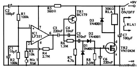
The circuit uses IC1 as a low-noise preamplifier with a voltage gain of 270 times. This is followed by a second stage of amplification, which produces a similar voltage gain. The second stage uses TR1 in the common-emitter mode; this is a conventional arrangement, except for the inclusion of C4. This capacitor provides a considerable amount of high-frequency attenuation, which is necessary in order to prevent instability. Capacitor C5 couples the greatly amplified output of TR1 to a rectifier and smoothing circuit, which gives a positive dc output signal that is roughly proportional to the input-signal level. If the input signal is sufficiently strong, the bias voltage at the gate of VMOS device TR2 will be adequate to bias this transistor into conduction, and the relay that forms its drain load is then activated, A pair of normally open relay contacts are used to control whatever item of equipment is operated by the unit. Of course, the voltage at the gate of TR2 soon decays, as C6 discharges through R8 if the input signal ceases, and the relay is then switched off. The decay time is roughly 1 second, which is about the optimum time for most applications. The attack time of the circuit is only a fraction of a second, and the unit responds almost immediately when a sound is initially picked up by the microphone. (View)
View full Circuit Diagram | Comments | Reading(0)
PIN_DIODE_TR_SWITCH
Published:2009/7/13 23:22:00 Author:May
Solid-state TR switch operates at very high keying speeds and handles up to 100 W while transferring antenna between receiver and transmitter in accordance with transmitter keying demands. Uses Unitrode UM4004 PIN diodes to provide about 0.2-dB insertion loss when forward-biased and about 30-dB isolation when reverse-biased. CR1 is forward-biased for about 45 mA DC and CR2 is reverse-biased by 124 V during transmit, for minimum loss in CR1 and maximum isolation in CR2. Circuit is designed to operate from collector of keying-circuit transistor in Touchcoder II (in dotted lines at lower left), but any source providing required T (transmit) and R (receive) DC voltages shown on diagram will key circuit. Article covers construction in detail.-J. K. Boomer, PIN Diode Transmit/Receive Switch for 80-10 Meters, Ham Radio, May 1976, p 10-15.
(View)
View full Circuit Diagram | Comments | Reading(2213)
TR_SWITCH
Published:2009/7/13 23:13:00 Author:May
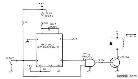
Simple transmit-receive switch uses 74122 retriggerable mono MVBR with clear and one NAND gate. When input of gate goes low (during key down or speech), transistor conducts and closes relay. Relay stays closed for period determined by delay pot, to maintain transmit condition between dots or dashes or between other pauses. Switch may be removed and any other TT'L-compatible input applied at point X.-B. Voight, The TI'L One Shot, 73Magazine, Feb, 1977, p 56-58. (View)
View full Circuit Diagram | Comments | Reading(0)
FULL_WAVE_CONTROL
Published:2009/7/13 23:13:00 Author:May
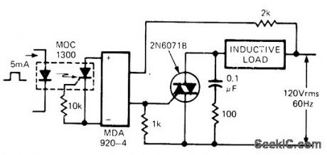
Uses triac to provide current for inductive load during both positive and negative alternations of AC source, with optoisolator providing complete isolation for logic control circuit. MDA920-4 diode bridge provides pulsating DC voltage for photo-SCR of optoisolator so gate current is supplied to triac for both halves of AC cycle.-T. Mazur, Solid-State Relays Offer New Solutions to Many Old Problems, EDN Magazine, Nov. 20,1973, p 26-32. (View)
View full Circuit Diagram | Comments | Reading(1877)
HALF_WAVE_AC_CONTROL
Published:2009/7/13 23:08:00 Author:May
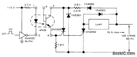
Motorola 4N26 optoisolator serves as interface for static series switch in gate circuit of 2N5064 SCR. When logic input goes high, optoisolator is energized and first SCR is triggered on. Resulting current turns on power SCR for passing load current on that positive half-cycle of AC line voltage. When logic goes low, load current stops at next zero crossing of AC source. 5mA of isolated DC control current thus controls up to 16 A for half-wave load.-A. Pshaenich, Interface Techniques Between Industrial Logic and Power Devices, Motorola, Phoenix, AZ, 1975, AN-712A, p 16. (View)
View full Circuit Diagram | Comments | Reading(2041)
| Pages:100/312 At 2081828384858687888990919293949596979899100Under 20 |
Circuit Categories
power supply circuit
Amplifier Circuit
Basic Circuit
LED and Light Circuit
Sensor Circuit
Signal Processing
Electrical Equipment Circuit
Control Circuit
Remote Control Circuit
A/D-D/A Converter Circuit
Audio Circuit
Measuring and Test Circuit
Communication Circuit
Computer-Related Circuit
555 Circuit
Automotive Circuit
Repairing Circuit