
Control Circuit
Index 97
TWO_TRANSISTOR_CURRENT_MODE_SWITCH
Published:2009/7/14 4:17:00 Author:May
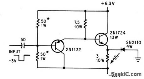
With two separate voltage supplies, input pulse triggers transistors to give 2-amp pulses for driving light-emitting diode.-F, .Bonin, Drivers for Optical Diodes, Electronics, 37:22, p 77-82. (View)
View full Circuit Diagram | Comments | Reading(964)
SWEEP_FOR_SSTV__MONITOR
Published:2009/7/15 4:59:00 Author:Jessie
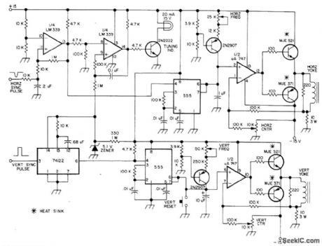
Uses two 555 timers. one as oscillator and other as linear sawtooth generator,Adjust R4 so oscillator period is slightly longer than interval between sync pulses. When sync is lost. oscillator runs very close to correct frequency and locks in again instantly on first good sync pulse. Circuit also has pulse stretcher, along with lamp driver that operates from horizontal sync pulses for use as tuning indicator,-R,L, Anderson. 555 Timer Sweep Circuit for SSTV 73 Magazine, May1976, p 134-136. (View)
View full Circuit Diagram | Comments | Reading(900)
LINEAR_TRUE_MEAN_SQUARE_TEMPERATURE_CONTROLLER
Published:2009/7/14 4:14:00 Author:May
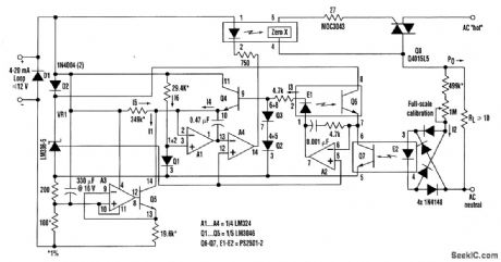
The power-control circuit shown outputs true-mean-square power in direct proportion to a 4- to 20-mA current-loop control input. The delivered power is tightly regulated, thus canceling line-voltage variations. In addition, it is proportioned on a fast 8.33-ms timebase, which avoids thermal ripple. The circuit operates as follows: 4- to 20-mA control inputs are converted by A3 and Q5 to negative 20 to 100μA (I1). I5 (fixed at±20 μA) zero-corrects I1, and the 0- to 80-μA difference is applied to the summing point of the A1 integrator. A4 compares the accumulated integral to a 2.5-V reference tapped from the ADJUST terminal of VR1 and, when the integral rises above that, it turns on the 3043 triac trigger optocouplen Zero-cross switching of the Q8 triac minimizes generated noise. Ac half-cycles through Q8 heat RI and push load-monitor current I2 through LED E2. To balance the resulting Q7 photocurrent, A2 produces I3, which causes matching conduction in the E1/Q6 optocoupler. Close tracking between sections of the 2501-2 dual optocoupler assures good proportionalitybetween I2 and I3 Because I3 also biases series-connected Q2 and Q3, voltage applied to the base of Q4 will be 2[X log (Y×I2)+Z], where X and Z are constants common to all five transistors in the 3046 monolithic array, and Y is set by the Fullscale Cal pot. As a result, antilog transistor Q4's emitter current is closely given by (Y ×12)2/I6. When integrated by A1, it gives an accurate prediction of the true-mean-square power dissipated in R1. The resulting feed-back loop acts to adjust Q8's duty cycle to regulate R1 power, allowing the temperature controller to accurately and linearly track the 4- to 20-mA control input signal. Operating power for the circuit is developed from the 4- to 20-rnA loop current, eliminating any need for another power source. (View)
View full Circuit Diagram | Comments | Reading(1102)
33_kW_SWITCHING
Published:2009/7/14 4:12:00 Author:May
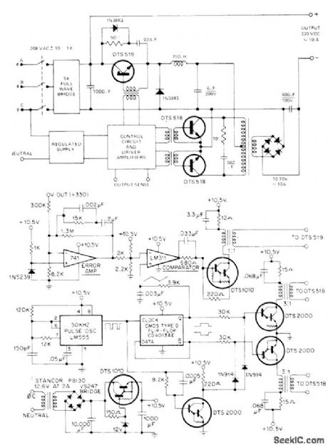
Delco DTS-518 and DTS-519 power transistors in high-efficiency stacked supply are operated at 25-kHz switching rate to provide 330 VDC at 10 A. Control circuit operates at primary 50-kHz pulse frequency, with negative-going pulses having 2-μs duration. Flip-flop converts this to 25-kHz complementary square-wave signal driving Darlington DTS-2000s. Transformer cores are Magnetics EE No. 42510 each having 15-tum primary and 5-tum secondary for driving DTS-518s. Error amplifier compares portion of total output voltage to zener reference for control of DTS-519 power transistor switching at 25 kHz. Efficiency is 95% at full Ioad.- 3.3kW High Efficiency Switch Mode Regulator, Delco, Kokomo, IN, 1977, Application Note 59. (View)
View full Circuit Diagram | Comments | Reading(961)
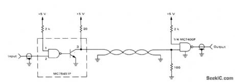
SINGLE_SUPPLY_LINE_DRIVER
Published:2009/7/15 4:53:00 Author:Jessie
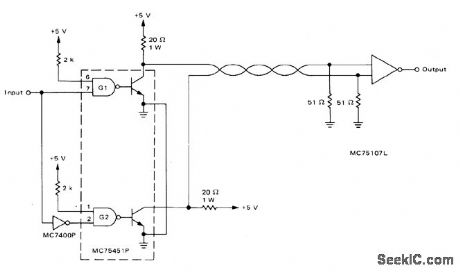
Motorola MC75451P driver and external components shown provide differential signal for twisted-pair transmission line from single +5 V supply. External gate provides required input phase reversal to gate G2 of IC. Each output ofIC varies between 0.5 V and 3.6 V, so net differential voltage driven into line is about 6 V. Only receiver end of line is terminated in its characteristic impedance, since arrangement is intended only for point-to-point transmission. -T. Hopkins, Line Driver and Receiver Considerations, Motorola, Phoenix, AZ, 1978, AN-708A, p 12. (View)
View full Circuit Diagram | Comments | Reading(852)
10_MHz_COAX_DRIVER
Published:2009/7/15 4:48:00 Author:Jessie
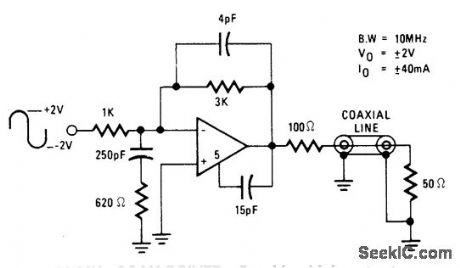
Provides high output current to coaxial line over bandwidth limited only by single-pole response of feedback components. Response is fiat with no peaking and distortion is low. Uses Harris HA-2530/2535 wideband amplifier having high slew rate.- Linear & Data Acquisition Products, Harris Semiconductor, Melbourne, FL, Vol, 1, 1977, p 7-54 (Application Note 516). (View)
View full Circuit Diagram | Comments | Reading(833)
VOLTAGE_CONTROL
Published:2009/7/14 4:09:00 Author:May
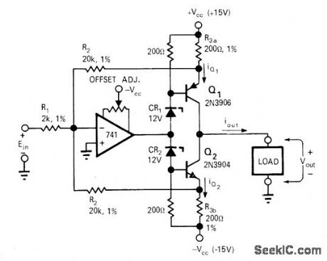
Improved voltage-con-trolled current source uses complementary transistors in opamp feedback loop. Common-mode voltage at input to opamp is always near zero. Circuit was designed for use in integrator having ground-referenced integrating capacitor, to produce 1 mA/V. R3a and R3b sense current through Q1 and Q2 so voltage proportional to difference is fed back to input of opamp for comparison with input voltage. Zener voltages determine quiescent-current level. Frequency response is limited to 1 MHz by performance of specified opamp.-P. T. Skelly, Voltage-Con-trolled Current Source, EDN/EEE Magazine, Aug. 1, 1971, p 45-46. (View)
View full Circuit Diagram | Comments | Reading(1977)
BIAS_SWITCH
Published:2009/7/14 4:01:00 Author:May
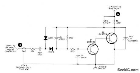
Automatic electronic bias switching improves efficiency of negatively biased linear class B RF power amplifier such as Heath SB-200 because no power is dissipated under no-signal conditions. Transistors are chosen to withstand maximum negative voltages switched, about -150 VDC. Capacitor across collector-base junction of Q1 can be adjusted to reduce turn-on time of switch. With no RE drive from transmitter, amplifier is biased to cutoff and plate current is zero. Switch will operate at RF threshold of about 2 V and apply class B bias voltage to amplifier. As RF drive is increased, plate current increases. With transmitter in SSB mode, plate current is zero with no speech. For speech, plate current increases with RF driving voltage.-F. E. Hinkle, Electronic Bias Switch for Negatively Biased Amplifiers, Ham Radio, Nov, 1976, p 27-29. (View)
View full Circuit Diagram | Comments | Reading(1768)
HALL_MULTIPLIER_PLATE_DRIVE
Published:2009/7/15 4:33:00 Author:Jessie
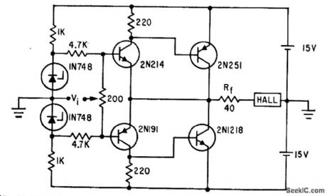
Currenl remains in phase with signal from 0 cps to over 20 kc. Distortion is less than 1% over entire range.-R. A. Greiner, Feedbock Amplification Improves Hall-Effect Multipliers, Electronics, 34:34, p 52-55. (View)
View full Circuit Diagram | Comments | Reading(781)
150_W_SWITCH_MODE
Published:2009/7/14 3:47:00 Author:May
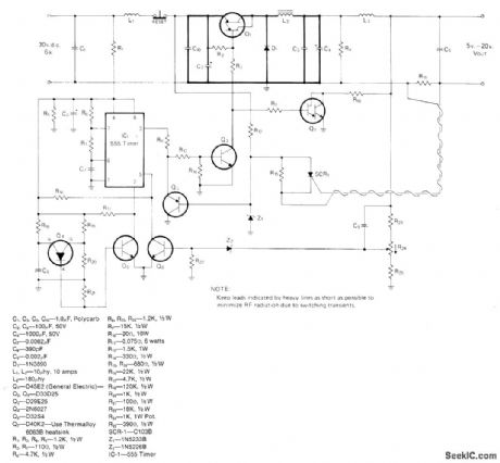
Unregulated DC voltage is applied to power Darlington Q1 serving as switch that chops voltage so rectangular waveform is applied to RLC output filter. Average voltage to filter depends on duty cycle of switch. 555 timer operates in mono MVBR mode as pulse generator and pulse-duration modulator. R24 applies varying voltage to pin 5 to modulate pulse duration linearly with respect to applied voltage, Actions of O1, Q2, and Q6 maintain constant 3.6 V at arm of control pot. Q4 and Q5 provide 20-kHz clock pulse, above audible range. Overcurrent protection of transistors is provided by R11, SCR, and Q3. Adjust R11 so SCR turns on and shuts down circuit when current through R11 reaches 8 A. Circuit must be reset manually after overload. Q7 and R10 load circuit to prevent oscillation at low output volt-age and light load.-R. J. Walker, A 150 Watt Switch-Mode Regulator, CQ, March 1977, p 40-43 and 74-75. (View)
View full Circuit Diagram | Comments | Reading(1073)
SCR_DRIVER
Published:2009/7/15 4:19:00 Author:Jessie
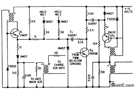
Two types of blocking oscillators generate required turn-on and turn-off pulses for power-switching output stage of inverter.-R. J. Kearns and J. J. Rolfe, Three .Phase Static Inverters Power Space-Vehicle Equipment, Electronics, 34:18, p 70-73. (View)
View full Circuit Diagram | Comments | Reading(1322)
SINGLE_ENDED_LINE_DRIVER
Published:2009/7/15 4:10:00 Author:Jessie
Supplies 4.2-V input pulse to twisted-pair transmission line for point-to-point system. Requires only single +5 V supply.-T. Hopkins, Line Driver and Receiver Considerations, Motorola, Phoenix, AZ, 1978, AN-708A, p14 (View)
View full Circuit Diagram | Comments | Reading(850)
5_kW_SWITCHING
Published:2009/7/14 3:49:00 Author:May
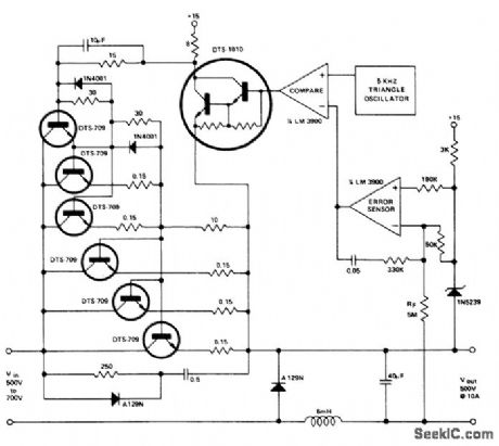
Six Delco DTS-709 transistors are connected in progressive Darlington configuration to provide stable and efficient switching at high voltages. Can be operated from 480-V three-phase full-wave rectified line to minimize filter cost. Control circuit uses one LM3900 IC operating from isolated 15-V supply, along with 5-kHz triangle oscillator and error sensor feeding into comparator. In power stage, one DTS-709 drives two DTS-709s which drive three DTS-709s. Efficiency is better than 90% for all loads above 500 W.- Economical 5 kW Switching Regulator Using DT'S-709 Transistors, Delco, Kokomo, IN, 1974, Application Note 56. (View)
View full Circuit Diagram | Comments | Reading(825)
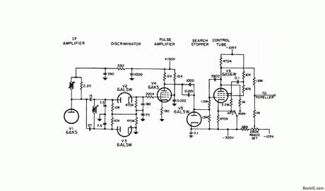
THYRATRON_AFC_FOR_AIRBORNE_RADAR_1
Published:2009/7/15 4:10:00 Author:Jessie
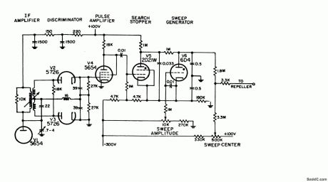
Uses Foster-Seeley discriminator to produce aeries of pulses varying from zero at crossover to maximum of 0.5 to 2 v at frequency of maximum response. Polarity may be either positive or negative, depending on whether incoming signal is above or below crossover frequency, and can be changed by reversing the diodes. Two thyratrons generate required control voltage for repeller of klystron.-NBS, Handbook Preferred Circuits Navy Aeronautical Electronic Equipment, Vol. 1, Electron Tube Circuits, 1963, p N 13-4. (View)
View full Circuit Diagram | Comments | Reading(1388)
DIFFERENTIAL_LINE_DRIVER
Published:2009/7/15 4:09:00 Author:Jessie
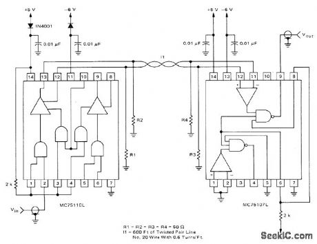
Uses Motorola MC75110L line driver and MC75107L receiver with twisted-pair transmission line having attenuation of 1.6 dB per 100 feet at 10MHz. Clock rate is 18.5 MHz. With push-pull driver shown, single pulse corresponds to transmission of 1 followed by series of 0s; one line is then at ground and the other at -300 mV. Arrangement is suitable for party-line or bus applications. -T. Hopkins, Line Driver and Receiver Considerations, Motorola, Phoenix, AZ, 1978, AN-708A, p 11. (View)
View full Circuit Diagram | Comments | Reading(1258)
POLARITY_NONREVERSING_DRIVE
Published:2009/7/15 4:07:00 Author:Jessie
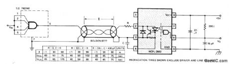
Packard HCPL-2602 optically coupled line receiver handles high data rates from shielded, twisted-pair, or coax cable fed by 745140 line driver, Reflections due to active termination do not affect performance. Peaking capacitor C and series resistor R can be added to achieve highest possible data rate. C should be as large as possible without preventing regulator in line receiver from turning off during negative excursions of input signal. Highest data rates are achieved by equalizing tPLH(propagation delay time to low output level) and tPHL (propagation delay time to high output level).- Optoelectronics Designer's Catalog 1977, Hewlett-Packard, Palo Alto, CA, 1977, p 158-159. (View)
View full Circuit Diagram | Comments | Reading(727)
CRYSTAL_DISCRIMINATOR_IN_AFC_LOOP
Published:2009/7/15 4:07:00 Author:Jessie
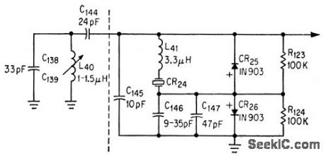
Gives narrow bandwidth at 23-Mc crystal frequency, for controlling drift of voltage controlled controlled oscillator.-F. L. Carroll, How to Achieve Stability in Space Telemetry, Electronics, 37:4, p 32-35. (View)
View full Circuit Diagram | Comments | Reading(796)
DIODE_PHANTASTRON_AFC_FOR_AIRBORNE_RADAR_1
Published:2009/7/15 4:05:00 Author:Jessie


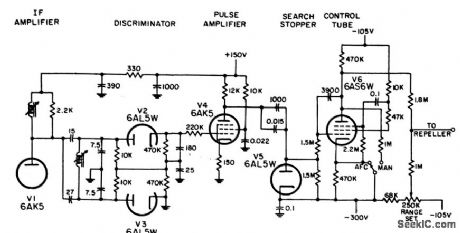
Pentode is astable phontastron during search and d-c amplifier during lock-on. Operation is nearly independent of tube characteristics. Provides tight control of local oscillator frequency because during lock-on, pentode furnishes direct control of klystron repeller.-NBS, Handbook Preferred Circuits Navy Aeronautical Electronic Equipment, Vol. 1, Electron tube Circuits, 1963, p N 13-6. (View)
View full Circuit Diagram | Comments | Reading(798)
PHANTASTRON_AFC
Published:2009/7/15 3:59:00 Author:Jessie
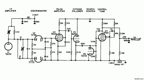
Pentode is astable phantastron during radar search, and d-c amplifier during lock-on when pentode furnishes direct control of klystron repeller.-NBS, Handbook Preferred Circuits Navy Aeronautical Electronic Equipment, Vol. 1, Electron Tube circuits, 1963,p N13-6 (View)
View full Circuit Diagram | Comments | Reading(1735)
5_V_SWITCHING
Published:2009/7/14 3:44:00 Author:May
Fixed OFF-time mode of operation is used in switching regulator design to provide 5-V output that is constant within 100 mV P-P for input range of 20-40 V, for loads ranging from 10 AL maximum to 2 A minimum. Switching frequency can be in range of 1-50 kHz. Operation above 20 kHz eliminates possibility of audio noise but with some drop in efficiency. Values shown are for 50 kHz. Article gives design equations and design procedure.-L. Dixon and R. Patel, Designers' LF Guide to: Switching Regulators, Part 2, EDN OUT Magazine, Nov. 5, 1974, p 37-40. (View)
View full Circuit Diagram | Comments | Reading(768)
| Pages:97/312 At 2081828384858687888990919293949596979899100Under 20 |
Circuit Categories
power supply circuit
Amplifier Circuit
Basic Circuit
LED and Light Circuit
Sensor Circuit
Signal Processing
Electrical Equipment Circuit
Control Circuit
Remote Control Circuit
A/D-D/A Converter Circuit
Audio Circuit
Measuring and Test Circuit
Communication Circuit
Computer-Related Circuit
555 Circuit
Automotive Circuit
Repairing Circuit