
Control Circuit
Index 95
LIGHT_OPERATED_TURNOFF_TOUCH_SWITCH
Published:2009/7/14 20:00:00 Author:May
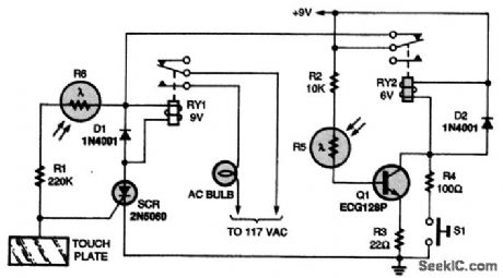
When R5 is illuminated by a flashlight, its resistance lowers, leaving only 10,000Ω as the minimum base resistance. That process gives a positive potential to the base of Q1, therefore turning on the transistor, activating RY2, and turning off the SCR. Or you can press S1 to turn the circuitry off. (View)
View full Circuit Diagram | Comments | Reading(897)
TOUCH_SWITCH_I
Published:2009/7/14 19:50:00 Author:May
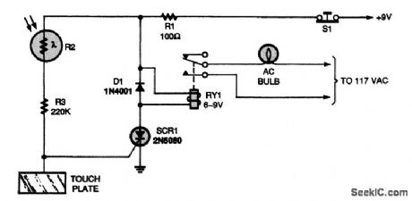
This touch switch controls an ac-powered bulb, and requires only a few parts. Touching the touch plate triggers the SCR's gate, turning it on and allowing current to flow from the cathode to the anode of SCR1, thereby activating the relay. (View)
View full Circuit Diagram | Comments | Reading(0)
GUITAR_TREBLE_BOOSTER
Published:2009/7/14 19:45:00 Author:May
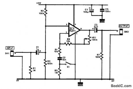
The circuit diagram shown was designed to increase the treble content of an electric guitar's output. It boosts frequencies above 1 kHz and helps to restore any higher-frequency losses. IC1 is a TL071 op amp connected as a noninverting amplifier, which is connected in the line between the guitar and the main amplifier. Potentiometer VR1 determines the level of treble boost applied; with the values of components shown, it will give between 3 and 20 dB. Resistor R6 and the potentiometer VR1 could be replaced by a fixed resistor, if required. The actual boost frequency is set by the values of resistor R4 and capacitor C2. With switch S1 open, the circuit acts as a voltage follower, with no effect on the guitar signal. Closing S1 grounds C2 to the 0-V line, which introduces the boost. Resistor R5 holds the earthy end of C2 at 0 V when switch S1 is open, and prevents switching noise appearing on the signal when S1 is operated. Resistors R2 and R3 set the input impedance of the circuit at 50 kΩ, which should suit most electric guitars. If the circuit is housed in a diecast case, S1 can be a foot-operated switch and SK1 could be a stereo jack socket with the sleeve and ring connections connected to the battery negative and 0-V rail, respectively. Thus, the unit will switch on automatically whenever the guitar is plugged in. Connect the case for the earth side of the circuit. Expect reasonable life from a PP3 battery. (View)
View full Circuit Diagram | Comments | Reading(3034)
INCANDESCENT_LAMP_TOUCH_CONTROL
Published:2009/7/14 12:18:00 Author:May
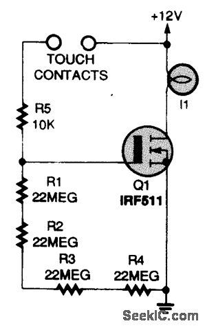
An IRF511 power MOSFET controls an incandescent lamp. This circuit is useful where low-voltage dc is used. (View)
View full Circuit Diagram | Comments | Reading(792)
ONE_BUTTON_LATCHING_SWITCH
Published:2009/7/14 12:13:00 Author:May

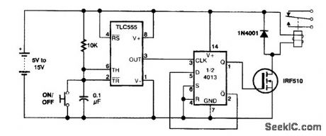
The SET and RESET inputs are grounded, the inverted (-Q) output is fed back to the D input, and the pulses go into the CLOCK input. Each positive pulse makes the flip-flop toggle from one state to the other. The TLC555 chip in the ftgure serves two purposes. It inverts the pulses so that you can get a positive pulse from a switch that is connected to ground. More importantly, it also debounces the switch. When you press a button, it doesn't just make contact once-the contacts bounce, opening and closing three or four times. The 4013 would toggle once on each bounce, leading to unpredictable results. Thp TLC555 uses a resistor and capacitor to smooth out these fluctuations so that each press of the button produces only one pulse. (View)
View full Circuit Diagram | Comments | Reading(2461)
LATCHING_SWITCH_CIRCUIT
Published:2009/7/14 12:06:00 Author:May
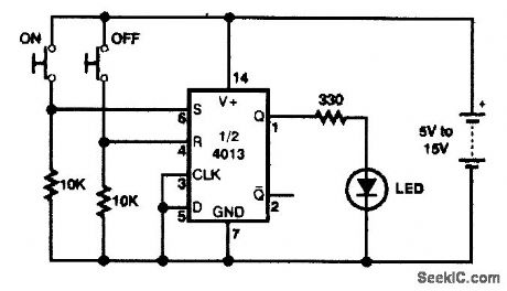
One button turns the LED on, the other turns it off. If you apply a positive pulse to the SET input, the output tums on. It remains on until a positive pulse is applied to the RESET input to turn it off. (TTL flip-flops such as the 74LS74 are actuated by negative, rather than positive pulses.) (View)
View full Circuit Diagram | Comments | Reading(2987)
400_Hz
Published:2009/7/15 2:05:00 Author:Jessie
One section of Signetics NE558 quad timer is used as nonprecision audio oscillator providing square-wave output of about 400 Hz with values and supply voltage shown. Output frequency is affected by changes in supply voltage.- Signetics Analog Data Manual, Signetics, Sunnyvale, CA, 1977, p 738.
(View)
View full Circuit Diagram | Comments | Reading(2100)
LASER_BEAM_ACTIVATED_RELAY
Published:2009/7/14 11:29:00 Author:May
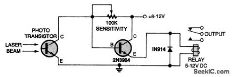
This two-transistor relay circuit will activate whenever the phototransistor is illuminated by the laser beam. (View)
View full Circuit Diagram | Comments | Reading(1869)
IR_RELAY_CIRCUIT
Published:2009/7/14 11:17:00 Author:May
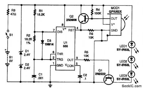
All IR is received by the module via an IR photodiode. The diode is operated in its reverse-bias current it permits depends on the intensity of the received infrared light. The fluctuations in the reverse-bias current are then amplified by a high-gain stage. The output of the amplifier is then limited by the next stage. The limiter chops the extreme highs and lows off the amplified signal, and the result is a quasi-digital pulse train. The simplified wave then passes through a bandwidth filter that has its center frequency at 40 kHz. At that point, the circuit has effectively retrieved the 40-kHz remote carrier. The reproduced carrier is then integrated. The next stage is an inverting Schmitt trigger. It will not go low unless the filter's output signal surpasses a certain amplitude, and it will not go high again until the signal drops below a certain minimum. Thus, the Schmitt trigger responds only to large changes in the filter's output (caused by bursts and pauses) and ignores small changes (caused by the 40-kHz carrier, to which the filter can't respond quickly). The Schmitt trigger's output is thus low when a 40-kHz burst is received, and high during pauses between bursts. The resulting waveform is an inverted version of the pulses that were modulated and transmitted by the remote. The oscillator circuit is based on a 555 timer. With D3, R2 is bypassed (or shorted out) while C1 is charging, but is in the current path during discharge. Therefore, with R1 and R2 made equal, the charge time equals the discharge time, yielding an output with a 50-percent duty cycle. Components R1, R2, and C1 (all precision, drift-free units) have been chosen to provide a 40-kHz output in this configuration. That output strobes the IR LEDs via Q1. The oscillator functions only when pin 4 of the 555 is high. Because that pin is connected to the inverter circuit, the oscillator functions when the inverter's input is low. The inverter's input is connected to MOD1's output, which goes low with each remote burst received. So overall, the circuit produces a 40-kHz IR burst when it receives one. (View)
View full Circuit Diagram | Comments | Reading(2077)
IR_REMOTE_CONTROL_MODEL_RAILROAD_APPLICATION
Published:2009/7/14 11:06:00 Author:May
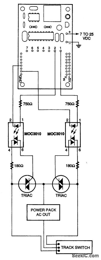
This circuit can be used to interface two triacs to the IR remote control in order to control model railroad track switches. (View)
View full Circuit Diagram | Comments | Reading(814)
IR_LOCAL_TALK_LINK_RECEIVER
Published:2009/7/14 8:13:00 Author:May

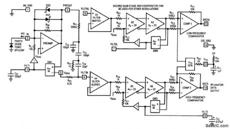
A low-noise (2 pA /√Hz),high-bandwidth (7 MHz) current-to-voltage converter formed by the preamplifier and its associated components transforms the reverse current from an external photodiode to a voltage. Although the 7-MHz bandwidth of the prearnp supports 4-Mbit data rates, a low-pass filter on the preamp output is used to reduce the bandwidth to just the required amount in order to reduce noise. As shown, capacitance CF1 sets the break frequency of an ac high-pass loop around the preamp to 180 kHz. This loop rejects unwanted ambient light, including sunlight and light from incandescent and fluorescent lamps. The preamp stage is followed by two separate channels, each containing a high-impedance filter buffer, two gain stages, high-pass loops, and a comparator. The only difference between the two channels is the response time of the comparators: 25 and 60 ns. For the 125-ns pulses of IR LocalTalk, the 25-ns comparator with its active pull-up output is used. The low-frequency comparator with its open collector output (with 5 kΩ internal pull-up) is suitable for more modest speeds, such as the 1.6-ps pulses or the IrDA-SIR. Each gain path has an ac coupling loop similar to the one on the preamp. Capacitance CF5 sets the high-pass comer at 140 kHz for IR LocalTalk. The loops serve the additional purpose here of maintaining an accurate threshold for the comparators by forcing the dc level of the differential gain stages to zero. As the preamp output is brought out and the inputs to the two comparator channels are buffered, the user is free to construct the exact filter required for the application by the careful selection of external components. RF1,CF2,CF3,RF4,CF4, and RF3 form a bandpass filter with a center frequency of 3.5 MHz and 3-dB points of 1 MHz and 12 MHz. Together with the high-pass ac loop in the preamp and the 7-MHz response of the preamp, this forms an optimal filter response for IR LocalTalk.
(View)
View full Circuit Diagram | Comments | Reading(845)
CONSTANT_CURRENT_CONTROL
Published:2009/7/14 5:38:00 Author:May
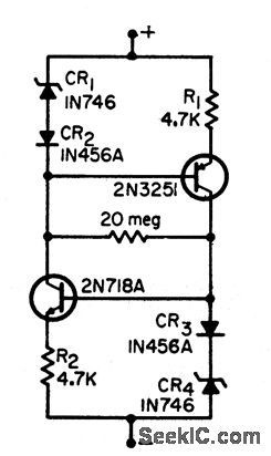
Uses pnp and npn current sources connected to regulate each other's reference. Values shown are for 1 ma, but R1 and R2 can be changed to give other constant value of current. Applied voltage must be at least 8V.-F. C. Allen, Two-Terminal Constant-Current Device, EEE, 13:10, p 71-72. (View)
View full Circuit Diagram | Comments | Reading(951)
BASS_BOOST_OR_LOUDNESS_CONTROL
Published:2009/7/15 2:35:00 Author:Jessie
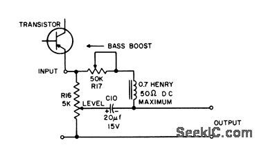
Operates on output of preamp.Gives operator independent control of level of bass or amount of bass boost desired. May also be used as loudness control.- Transistor Manual, Seventh Edition, General Electric co.,1964,p 254. (View)
View full Circuit Diagram | Comments | Reading(3821)
CURRENT_REGULATOR_FOR_0_100_MA
Published:2009/7/14 5:40:00 Author:May
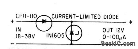
Constant. current Currector diode and shunting zener diode together maintain constant current over extremes of input voltage for both normal and shorted loads.-N. Wejsh, How Diodes Keep Current to Constant Value, Electronics, 36:4, p 74-78. (View)
View full Circuit Diagram | Comments | Reading(828)
TONE_CONTROL
Published:2009/7/15 2:12:00 Author:Jessie
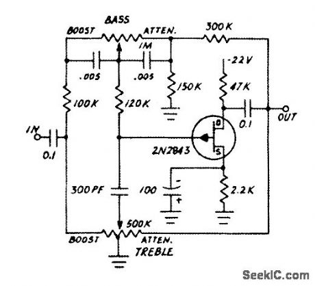
Unlike bipolar transistor, fet maintains full dynamic range whileloading R.C tone control network.-FET's and RC Networks (Siliconix ad), Electronics,39:4, p 71. (View)
View full Circuit Diagram | Comments | Reading(2276)
5_V_SWITCHING_1
Published:2009/7/14 4:41:00 Author:May
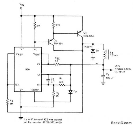
Darlington pair Q1-Q2 serves as switch for regulator using Signetics 550 as threshold detector. Design equations are given. Exact frequency of self-oscillating switching regulator depends primarily on parasitic components. If frequency is important, as in applications requiring EMI suppression, regulator may be locked to external square-wave drive signal fed to reference terminal.- Signetics Analog Data Manual, Signetics, Sunnyvale, CA, 1977, p 661-662. (View)
View full Circuit Diagram | Comments | Reading(911)
START_UP_CONTROL
Published:2009/7/14 4:43:00 Author:May
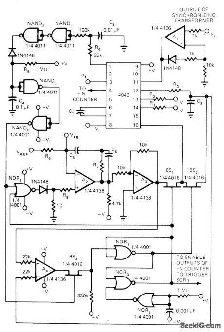
Simple, smooth start-up circuit for phase-locked oscillator maintains synchronism with AC line despite presence of large transients, and maintains phase-angle limits as required for controlling firing angle of SCR. Article describes how two separate loops are used in circuit to achieve required locking with line. Values of R6, R7, R8, C5, and C6 are chosen to meet system response time, Other unmarked values depend on operating factors; for 60-Hz line and 6X frequency multiplication by VCO, typical values are R1 39K, R2, 27K, R3 47K, C1 0.1μF, and C2 0.22μF.-J. C. Hanisko, Five IC's Make Ainsworth Oscillator with Start-Up Control, EDN Magazine, March 5, 1977, p 113 and 115. (View)
View full Circuit Diagram | Comments | Reading(1342)
CROWBAR
Published:2009/7/14 5:32:00 Author:May
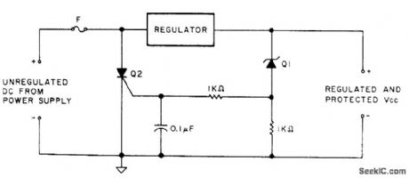
When output of regulator for microprocessor power supply exceeds maximum safe voltage as determined by zener Q1, SCR Q2 is triggered on and conducts heavily, blowing fuse rapidly to protect equipment. Fuse rating is 125% of nominal load. Choose SCR to meet voltage and current requirements. Choose zener for desired trip voltage. Each germanium diode in series with Q1 will add 0.3 V to trip voltage, and silicon diodes add 0.6 V. To calibrate, place 1K resistor temporarily in series with Q2 and measure drop across it to see if SCR fires and produces surge on meter at desired VCC.-J. Starr, Want to Buy a Little Insurance? , Kilobaud, 0ct. 1978, p 89. (View)
View full Circuit Diagram | Comments | Reading(0)
COLLECTOR_CAPACITORS_SPEED_SWITCHING_
Published:2009/7/15 3:20:00 Author:Jessie
Capacitors acting with 3-ohm resistors in collector circuits provide energy storage to increase switching speed.-A. G. Lloyd, Speed-Up Circuits Improve Switching of Transistor Inverters, Electronics, 34:45, p 92-94. (View)
View full Circuit Diagram | Comments | Reading(784)
BINARY_CONTROL_OF_GAIN
Published:2009/7/14 5:09:00 Author:May
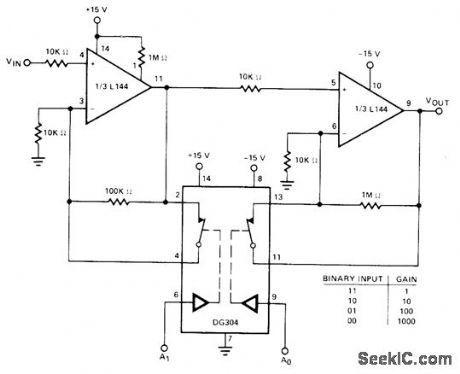
Gain of amplifier increases by decades from 1 to 1000 as binary input to A1 and A0 of DG304 low-power analog switch decreases from 1,1 to 0,0. Power dissipation of switch is less than 0.1 mW.- Analog Switches and Their Applications, Siliconix, Santa Clara, CA, 1976, p 7-86. (View)
View full Circuit Diagram | Comments | Reading(779)
| Pages:95/312 At 2081828384858687888990919293949596979899100Under 20 |
Circuit Categories
power supply circuit
Amplifier Circuit
Basic Circuit
LED and Light Circuit
Sensor Circuit
Signal Processing
Electrical Equipment Circuit
Control Circuit
Remote Control Circuit
A/D-D/A Converter Circuit
Audio Circuit
Measuring and Test Circuit
Communication Circuit
Computer-Related Circuit
555 Circuit
Automotive Circuit
Repairing Circuit