
Control Circuit
Index 101
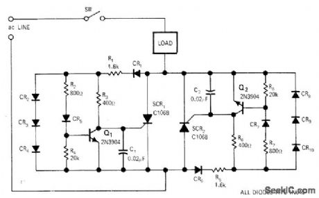
PROTECTION_AGAINST_SIMULTANEOUS_OPERATION_OF_TRIACS
Published:2009/7/13 22:48:00 Author:May
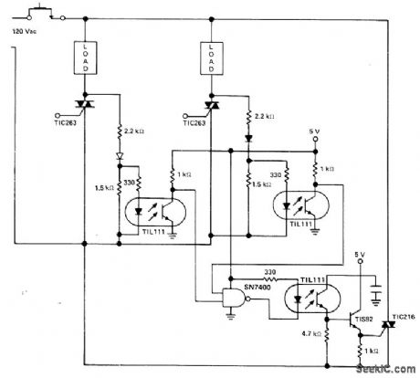
Optoisolators provide cross-connection between solid-state triac relay circuits to eliminate possibility that two or more triacs come on at same time due to circuit malfunction or component failure. Circuit shuts system down when this occurs.- Thyristor Gating for μP Applications,″ Texas Instruments, Dallas, TX, 1977,CA-191,p 5-9. (View)
View full Circuit Diagram | Comments | Reading(1799)
ZERO_POINT_SWITCH
Published:2009/7/13 22:44:00 Author:May
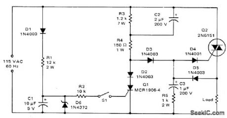
Used to control resistive loads. With S1 open, triac Q2 is turned on very close to zero on initial part of positive half-cycle because of large current flow into C2.Once Q2 is on, C3 charges through D5. When line voltage goes through zero and starts negative, C3 is still discharging into gate of C2 to turn it on near zero of negative half-cycle. Load current thus flows for most of both half-cycles. When S1 is closed, Q1 is turned on and shunts gate current away from Q2 during positive half-cycles. Q2 cannot turn on during negative half-cycle because C3 cannot charge, which makes load current zero.- Circuit Applications for the Triac, Motorola, Phoenix, AZ, 1971, AN-466, p 12. (View)
View full Circuit Diagram | Comments | Reading(0)
TTL_INTERFACE_FOR_VMOS
Published:2009/7/13 22:32:00 Author:May
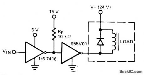
By using opencollector 7416 TTL interface with its output pulled up to 15V,S55V01 VMOS will switch up to 2 A easily. Inductive load such as relay requires diode across relay coil-L. Shaeffer, VMOS Peripheral Drivers Solve High Power Load Interface Problems, Computer Design,Dec.1977,p 90,94,and 96-98.
(View)
View full Circuit Diagram | Comments | Reading(790)
TR_SWITCH
Published:2009/7/13 22:28:00 Author:May
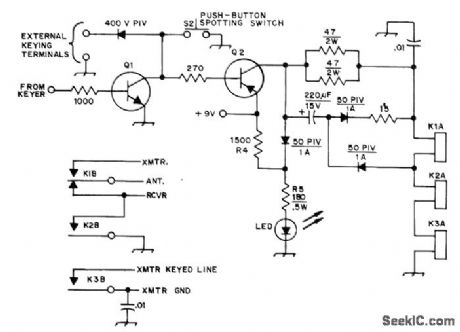
Consists of driver transistors Q1 and Q2 and reed relays K1-K3. K1 switches antenna from receiver to transmitter, K2 grounds receiver input, and K3 keys transmitter. Coil of K1 has 400 turns No. 32 enamel, while K2 and K3 each have 120 tums. Coils are wound directly on glass of reed relays and covered with epoxy cement. LED normally glows dimly, with brightness increasing when character is keyed.-J. H. Fox, An Integrated Keyer/TR Switch, QST, Jan. 1975, p 15-20. (View)
View full Circuit Diagram | Comments | Reading(1473)
125_ns_POWER_SWITCH
Published:2009/7/13 22:13:00 Author:May
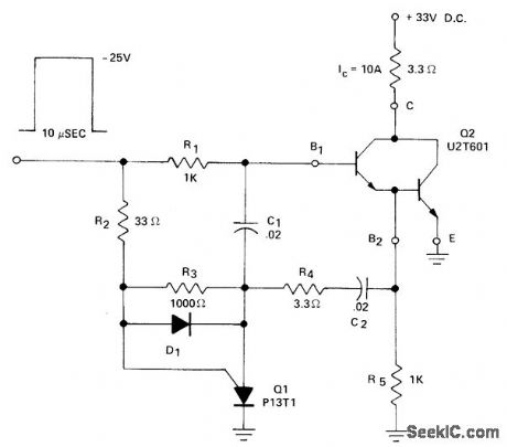
Developed for repetitive pulse applications in which rise, fall, and storage times of pulse must be kept at absolute minimum. Circuit provides very high gain of Unitrode U2T601 Darlington and switching speeds up to 5 times greater than conventional techniques. Load power up to 10 A is typically applied within 125 ns. Applications include drive for laser diode and for radar circuits.- Designer's Guide to Power Darlingtons as Switching Devices, Unitrode, Watertown, MA, 1975, U-70, p 19. (View)
View full Circuit Diagram | Comments | Reading(750)
TIME_DELAYED_MODEL_ROCKET_LAUNCH_CONTROL
Published:2009/7/13 22:07:00 Author:May
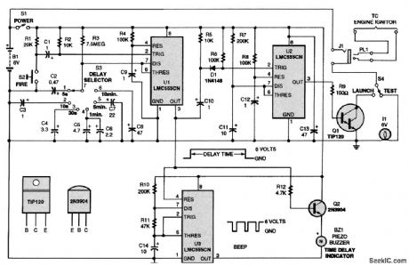
The circuit, which gives a choice of six delay settings, consists of three 555 oscillator/timers (U1 to U3), a pair of transistors (Q1 and Q2), four switches (S1 to S4), a piezoelectric buzzer (BZ1), and a few support components. Power for both the control circuit and the rocket-engine igniter is provided by a 6-V power source that is composed of four AA-cell alkaline batteries. Closing switch S1 feeds power to the launch-control circuit, but does not initiate a launch sequence. A pair of series RC circuits(R4-C9 and R8-C12, respectively) are used to debounce the RESET inputs (pins 4) of U1 and U2 (a pair of 555 oscillator/timer ICs). When S2 is closed, C1's negative terminal is connected to ground through the switch, momentarily pulling pin 2 of U1 (which is configured as a monostable multivibrator, or one-shot) low, activating it. Once triggered, U1's output goes high for an interval that is determined by R3 and one of six timing capacitors (C2 through C8). The timing capacitor is selected via DELAY SELECTOR switch S3. The high output of U1 at pin 3 causes Q2 to turn on, allowing the piezoelectric buzzer BZ1 to turn on. Monostable U1's output is also fed to the RESET input of U3 at pin 4, causing it to oscillate with a duty cycle of about 75 percent. As long as the output of U1 is high and the astable is oscillating, BZ1 beeps once every 4 s. The resistor discharges coupling capacitor C10 whenever U1's output goes high. At the end of the selected time delay, U1's output goes low.That low is coupled through C10 and D1 to the TRIGGER input (pin 2) of U2. Components R7 and C11 set U2's high-output interval to approximately 3 s. During that 3-s interval, U2's high output at pin 3 is fed to Darlington transistor Q1 through R9. With S4 in the LAUNCH position, Q1 grounds one end of the engine igniter, effectively connecting it to the battery's negative terminal. (View)
View full Circuit Diagram | Comments | Reading(3606)
FULL_WAVE_AC_CONTROL
Published:2009/7/13 22:04:00 Author:May
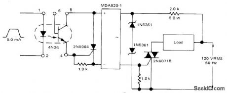
Motorola type MDA920-1 bridge rectifier provides full-wave rectification of AC line voltage for 2N5064 SCR placed across DC output of bridge. When positive logic pulse from CMOS circuit energizes optoisolator, SCB conducts and completes path for triac gate trigger current through bridge and SCR, turning on AC load. Triac rating determines size of load. Drawback of circuit is generation of EMI if logic signal occurs at other than zero crossings of AC line.-A. Pshaenich, Interface Techniques Between Industrial Logic and Power Devices, Motorola, Phoenix, AZ, 1975, AN-712A, p 17. (View)
View full Circuit Diagram | Comments | Reading(1737)
FULL_WAVE_POWER_CONTROL
Published:2009/7/13 21:46:00 Author:May
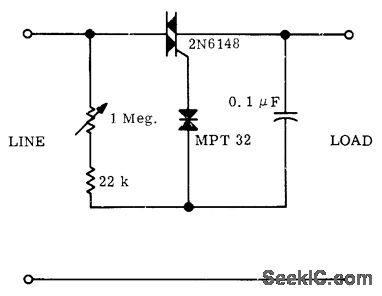
Bidirectional three-layer trigger for triac allows triggering on both half-cycles at point determined by setting of 1-megohm pot. Triac rating determines size of load that can be handled.- SCR Power Control Fundamentals, Motorola, Phoenix, AZ, 1971, AN-240, p 6.
(View)
View full Circuit Diagram | Comments | Reading(787)
AUTO_SECURITY_DEVICE_1
Published:2009/7/13 21:44:00 Author:May
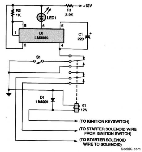
Combining two functions in one, this circuit is both a passive cutoff device and a fake car alarm Depressing S1 with the key in the RUN position disables the flasher and allows the car to start. (View)
View full Circuit Diagram | Comments | Reading(770)
LINE_POWERED_SWITCH
Published:2009/7/13 21:43:00 Author:May
When AC line twitch is closed, power is not applied to load until after line voltage next goes through zero. Identical circuits control each half of AC cycle. Transistor turn-on at 1.4 V prevents SCR from triggering until 0.013 ms (less than one-third electrical degree) after next zero-crossing point.-A. S. Roberts and O. W. Craig, Efficient and Simple Zero-Crossing Switch, EDN|EEE Magazine, Aug. 15, 1971, p 46-47. (View)
View full Circuit Diagram | Comments | Reading(824)
TR_CONTROL
Published:2009/7/13 21:43:00 Author:May

Used to control low-power transceiver for 20-meter amateur band. Sidetone is obtained from simple relaxation oscillator using GED-13-T programmable UJT. Sawtooth output is attenuated and applied to input of two-transistor audio amplifier. Transmitter keying is done with series switch using 2N4036 silicon transistor. Antenna relay applies +12 V appropriately to transceiver stages used during transmit (+12T) and receive (+12R), and provides switching of antenna between transmitter power chain and receiver RF amplifier. Use DPDT relay with 800-ohm 12-V coil. Transmit receive logic uses μA741C opamp as differential comparator. When key is closed, 2.2-μF capacitor is discharged, making opamp output switch to high state and saturate 2N3904 relay driver, pulling in relay for transmit operation. When key is released, capacitor begins to charge; at 6-V point (about 0.5 s with 220K timing resistor), opamp changes state again and relay opens for receiving.-W. Hayward, Low-Power Single Band CW Transceiver, Ham Radio, Nov. 1974, p 8-17. (View)
View full Circuit Diagram | Comments | Reading(906)
SLICER_AND_GATE_FOR_AGC
Published:2009/7/16 2:33:00 Author:Jessie
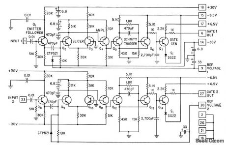
When peak-to-peak value of input signal exceeds preset reference voltage, slicer Q2 conducts, making Q4 apply amplified signal to Schmitt trigger for squaring. Q7 then delivers output ate that changes fixed-gain amplifier to unity gain to give effect of fast agc for monopulse radar amplifier.- W. W. Smith, Fast AGC Amplifier Locks Monopulse Radar on Target Electronics, 36:39, p 34-36. (View)
View full Circuit Diagram | Comments | Reading(758)
BRIDGE_TRIGGERED__TRIAC
Published:2009/7/13 21:41:00 Author:May
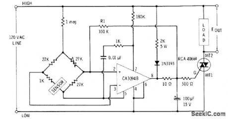
Developed for use with AC sensor in one leg of bridge. CA3094 is shut down on negative half-cycles of line. When bridge is unbalanced so as to make pin 2 more positive than pin 3, IC is off at instant that AC line swings positive; pin 8 then goes high and drives triac into conduction. Triac conduction is maintained on next negative half-cycle by energy stored in 100-μF capacitor. Bridge unbalance in opposite direction does not trigger triac.-E. M. Noll, Linear IC Principles, Experiments, and Projects, Howard W, Sams, Indianapolis, IN, 1974, p 313-314. (View)
View full Circuit Diagram | Comments | Reading(1020)
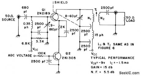
30_MC_GAIN_CONTROLLED_STAGE
Published:2009/7/16 2:31:00 Author:Jessie
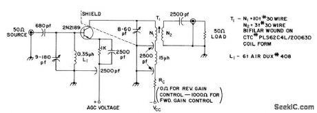
Gain is 15db. Typical noise figure is 5db. Reverse gain control range is 25 db from collector current of 1.5 ma to 20 microamp. Provides 20 db of forward gain control.- Texas Instruments Inc., Solid-State Comunications, McGraw-Hill,N.Y.,1966, p 211. (View)
View full Circuit Diagram | Comments | Reading(706)
30_MC_GAIN_CONTROLLED_TETRODE
Published:2009/7/16 2:29:00 Author:Jessie
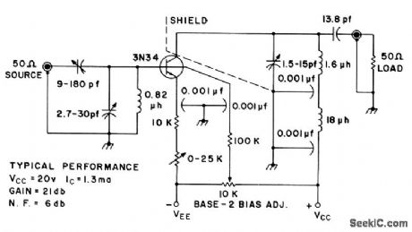
Collector voltage and current are kept constant and gain is changed in accordance with base-2 current. Gain is 21 db and typical noise figure is 6O db,-Texas Instruments Inc., Solid-State Communications, McGraw-Hill, N.Y., 1966,p 213. (View)
View full Circuit Diagram | Comments | Reading(758)
BACK_PORCH_KEYED_AGC
Published:2009/7/16 2:28:00 Author:Jessie
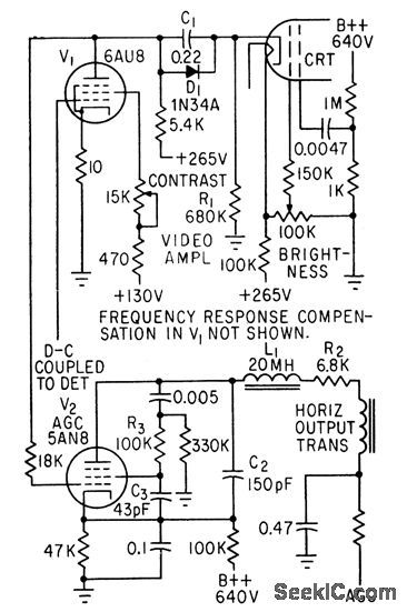
Composite of d-c coupling for dark scenes and a-c coupling for bright scenes, with agc referenced to back-porch (blanking level) rather than to sync tips, approaches ideal compromise for automatic control of tv picture.-L. Solomon, New Tubes and Circuits for Consumer Electronics, Electronics, 36:2, p 47-49. (View)
View full Circuit Diagram | Comments | Reading(770)
SIGNAL_LEVEL_CONTROLS_GAIN
Published:2009/7/16 2:25:00 Author:Jessie
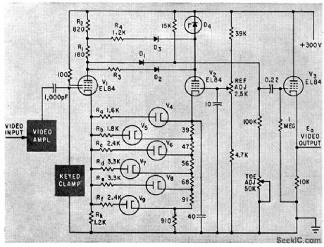
Amplifier is used with nonlinear circuit elements to gel D-versus-log E characteristic approximating that of positive color film being scanned. When no signal is applied to grid of V1, all diodes in its cathode circuits are conducting, equivalent cathode resistance is lowest, and stage gain is highest. As signal level increases, diodes V4 through V9 successively stop conducting, with V9 turning off last to make stage gain a minimum.-R. lid. Farber and K. M. St. John, Scanner Analyzes Color Content of Movie Film, Electronics, 34:48, p 38-41. (View)
View full Circuit Diagram | Comments | Reading(709)
30_MC_HYBRID_GAIN_CONTROL
Published:2009/7/16 2:24:00 Author:Jessie
Q2 acts as variable impedance to give emitter degeneration, which is a form of external gain control. Q2 also controls collector current of Q1 to give reverse gain control action, which is internal gain control. Gain control range is 33 db, with 2:1 change in bandwidth.-Texas Instruments Inc., Solid-State Communications, McGraw-Hill, N.Y., 1966, p 222. (View)
View full Circuit Diagram | Comments | Reading(781)
450_MC_GAIN_CONTROLLED_STAGE
Published:2009/7/16 2:22:00 Author:Jessie
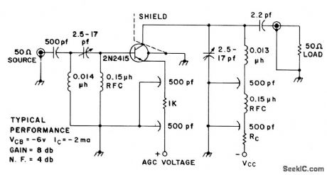
Has gain of 8 db with typical noise figure of 4 db. Reverse gain control is 21 db for collector current of 20 microamp, and forward gain control is 26 db at 7 ma collector current.-Texas Instruments Inc., Solid-State Communications, McGraw-Hill, N.Y., 1966, p 220. (View)
View full Circuit Diagram | Comments | Reading(675)
AUDIO_AGC_FOR_40_DB_RANGE
Published:2009/7/16 2:20:00 Author:Jessie
Automatic gain-adjusting amplifier produces constant output for speech level variations up to 40 db. Intelligibility of speech is ensured by allowing instantaneous peaks to remain.-L.E. Getgen, Amplifier Compensates for Speech-Level Variations, Electronics,33:31, p 103-106. (View)
View full Circuit Diagram | Comments | Reading(749)
| Pages:101/312 At 20101102103104105106107108109110111112113114115116117118119120Under 20 |
Circuit Categories
power supply circuit
Amplifier Circuit
Basic Circuit
LED and Light Circuit
Sensor Circuit
Signal Processing
Electrical Equipment Circuit
Control Circuit
Remote Control Circuit
A/D-D/A Converter Circuit
Audio Circuit
Measuring and Test Circuit
Communication Circuit
Computer-Related Circuit
555 Circuit
Automotive Circuit
Repairing Circuit