
Control Circuit
Index 118
SELF_LATCHING_BURGLAR_ALARM
Published:2009/7/9 21:31:00 Author:May
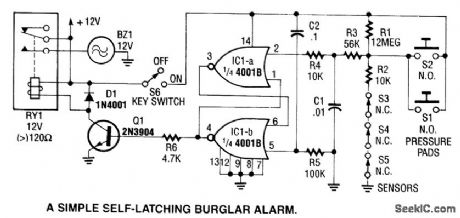
This alarm uses IC1A and IC1B as a latch. When sensors S1 through S5 activate, IC1A turns on and forces IC1B to cut off. Q1 drives RY1. (View)
View full Circuit Diagram | Comments | Reading(941)
PROXIMITY_SWITCH
Published:2009/7/9 21:29:00 Author:May
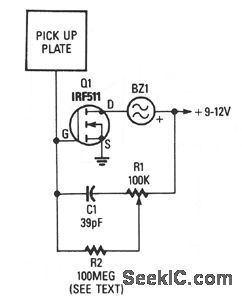
A 3- x -3-inch piece of circuit board, or similar size metal object which functions as the pick-up sensor, is connected to the gate of Q1. A 100-MΩ resistor, R2, isolates Q1's gate from R1, allowing the input impedance to remain very high. If a 100-MΩ resistor cannot be located, just tie five 22-MΩ resistors in series and use that combination for R2. In fact, R2 can be made even higher in value for added sensitivity.Potentiometer R1 is adjusted to where the piezo buzzer just begins to sound off and then carefully backs off to where the sound ceases. Experimenting with the setting of R1 will help in obtaining the best sensitivity adjustment for the circuit.Resistor R1 can be set to where the pick-up must be contacted to set off the alarm sounder. A relay or other current-hungry component can take the place of the piezo sounder to control most any extemal circuit. (View)
View full Circuit Diagram | Comments | Reading(0)
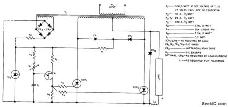
CAPACITIVE_SENSOR_ALARM
Published:2009/7/9 21:24:00 Author:May
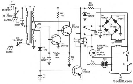


The unit is constructed around a balanced-bridge circuit, using both capacitance and inductance. The bridge consists of capacitors C2 and C3, and the center-tapped winding of T1. One end of the bridge is coupled to ground by C4, while capacitance changes are introduced through C1. A small capacitance change unbalances the bridge and produces an ac signal at the base of Q1. Transistors Q1 and Q2 are connected to form a modifted-Darlington amplifier. The collector load for Q2 is a separate winding of T1 that is connected out-of-phase with the incoming ac signal. That produces a large, distorted signal each time the bridge is unbalanced.The distorted signal is taken from the bridge circuit by a third winding of transformer T1. That signal is then rectified by D6 and applied as a dc signal to the base of Q3. The applied signal energizes the relay, K1, as soon as the unbalanced condition occurs, and the relay drops out as soon as the circuit balance is restored. Of course, for normal alarm use, the relay should be made self-latching, so that the alarm condition remains in effect until the system is reset.An audible alarm, such as a bell or klaxon horn, can be operated from the relay. If a silent alarm is needed, a light bulb can be used. Transformer T1 can be purchased as part #6182 from: Pulse Engineering, P.O. Box 12235, San Diego, CA 92112. (View)
View full Circuit Diagram | Comments | Reading(1257)
FAST_OVERVOLTAGE_PROTECTOR
Published:2009/7/9 21:21:00 Author:May


This circuit protects expensive portable equipment against all types of improper hookups and environmental hazards that could cause an overvoltage condition. It operates very quickly and does not latchup, that is, it recovers when the overvoltage condition is removed. In contrast, SCR overvoltage circuits can latch and do not recover, unless the power is removed.Here, U1 senses an overvoltage condition when the drop across R1 exceeds 2.5 V. This causes U1 to apply a positive signal to the gate of Q1, turning it on and shorting the line going to the external circuits. Fuse 1 opens if the transient condition lasts long enough to exceed the i2t rating. (View)
View full Circuit Diagram | Comments | Reading(1178)
POWER_FAILURE_ALARM
Published:2009/7/9 21:17:00 Author:May
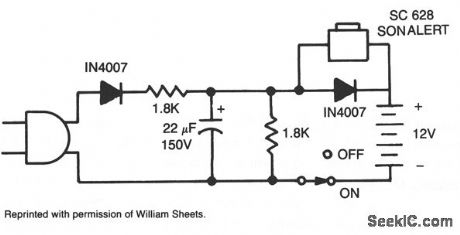
With power ac off, the alarm sounds when S1 is closed on. The 12-V battery is kept charged when the circuit is plugged in and the switch is left on. (View)
View full Circuit Diagram | Comments | Reading(0)
PHASE_MEASURING_AT_30_MC
Published:2009/7/20 4:19:00 Author:Jessie
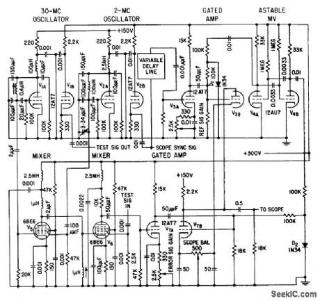
Double mixing process linearly transposes phase shifts accumulated at 30 Mc down to 2 Mc, where they are accurately compared against calibrated 2-Mc reference signal. Samples of 30-Mc and 2-Mc signals are mixed in V5, and 32-Mc sum frequency is then mixed with phase-shifted 30-Mc signal from unit under test by V6. Difference frequency, equal to 2 Mc plus phase shift, is amplified in V7A, fed through gate V7B, and associated circuits then superimpose this signal and that of 2-Mc reference oscillator on cro to get display of phase shift.-A. Nirenburg, How to Measure Midfrequency Phase Shift, Electronics, 31:35, p 46-47. (View)
View full Circuit Diagram | Comments | Reading(637)
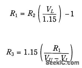
NONLATCHING_RELAY
Published:2009/7/9 21:03:00 Author:May
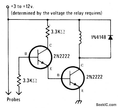
When liquid rises above level determined by positions of probes, circuit is triggered and relay, buzzer, or other indicator is energized. Alarm stops when liquid drops below preset level again. Use any operating voltage from 3 to 12 V that will actuate load employed.-J. A. Sandier, 9 Easy to Build Projects under $9, Modern Electronics, July 1978, p 53-56. (View)
View full Circuit Diagram | Comments | Reading(1241)
DIGITAL_PHASE_METER
Published:2009/7/20 4:00:00 Author:Jessie
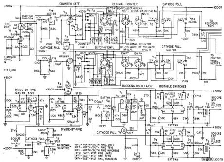
Measures phase angle between satellite signal and reference pulse. Bistable switch operates as gate that connects 500-cps pulse train to 3-decade decimal counter during time between reference and signal pulses. Two channels measure phase angles of north-south and east-west fine signals.-C. A. Schroeder, C. H. Looney, Jr., and H. E. Carpenter, Jr., Tracking Orbits of Man-made Moons, Electronics, 32:1, p 33-37. (View)
View full Circuit Diagram | Comments | Reading(1287)
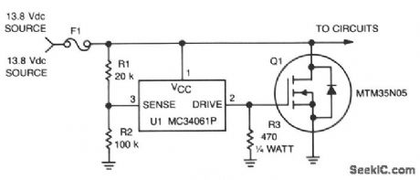
BATTERY_SAVING_DISCONNECT_SWITCH
Published:2009/7/9 20:52:00 Author:May
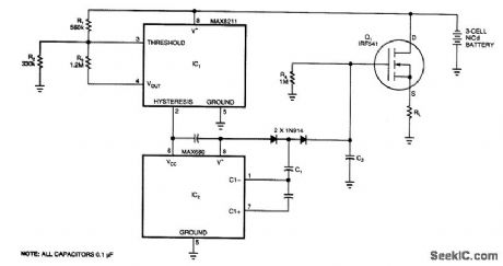


At a predetermined level of declining terminal voltage, the circuit disconnects the battery from the load and halts potentially destructive battery discharge. Q1, a high-side, floating-source MOSFET, acts as the switch. The overall circuit draws about 500 μA when the switch is closed and about 8 μA when it's open.
The values of Ry, R2, and R3 set the upper and lower voltage thresholds, Vu and Vy,, according to the relationships
For the circuit to start,V+ must exceed Vu. The voltage detector IC1 then powers IC2, but only while V+ remains above VL. Otherwise, IC2 loses its power, removes gate drive from Q1, and turns it off. IC2 is a dual charge-pump inverter that normally converts 5 V to ±10 V. Capacitors C1, C2, and the two associated diodes form a voltage tripler that generates a gate drive for Q1 that is approximately equal to two times the battery voltage.
With the values in the schematic, the circuit disconnects 3-cell Nicad battery from its load when V+ reaches a VL of 3,1 V. Approximately 0.5 V of hysteresis prevents the switch from turning on immediately when the circuit removes the load; V+ must first return to Vu, which is 3.6 V. The gate drive declines as the battery voltage declines, cause the ON-resistance of Q1 to reach a maximum of approximately 0.1 Ω, just before Y+ reaches its 3.1-V threshold. A 300-mA load current at that time will cause a 30-mV drop across the disconnect switch, The drop will be 2 to 3 mV less for higher battery voltages. Resistor R4 ensures that Q1 can adequately turn off by providing a discharge path for C2. (View)
View full Circuit Diagram | Comments | Reading(1290)
IR_REFLECTION_PROXIMITY_SWITCH
Published:2009/7/9 20:50:00 Author:May
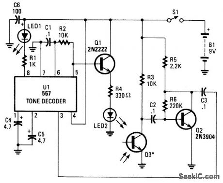
IR radiation from LED2 (modulated by a 1-kHz wave) is keyed by U1, and Q1 is radiated. Reflected IR energy is picked up by Q3, and the audio signal from Q3 is amplified by Q2 and sent to the decoder. The LED1 lights to indicate presence of reflected IR. LED1 can be the input of an isolator so that a triac or SCR can be controlled. (View)
View full Circuit Diagram | Comments | Reading(1083)
FIRING_ANGLE_CONTROL
Published:2009/7/20 4:59:00 Author:Jessie
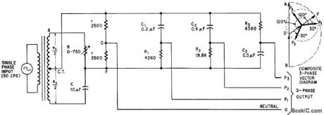
Varying R from 0 to infinity shifts the three phase voltages from 0° to 180°.-J. J. Vithayathil, Variable-Phase, Polyphase From Single-Phase Supply, Electronics, 37:27, p 56-57. (View)
View full Circuit Diagram | Comments | Reading(751)
INFRARED_REMOTE_CONTROLLER
Published:2009/7/9 20:32:00 Author:May
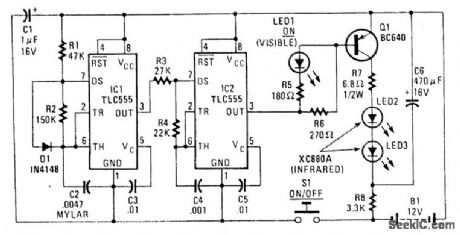
The transmitter is built around two CMOS 555 timer ICs (TLC 555s). The transmitter generates a modulated 35-kHz IR signal. The 35-kHz carrier frequency is generated by IC2, and the 1 500-Hz modu-lating signal is generated by IC1. The output of IC2 drives LED1 through resistor R5; that LED provides visual indication that the transmitter is working. In addition, IC2 drives transistor Q1, which drives the two infrared LEDs (LED 2 and LED3).
To provide the high current needed to drive the two IR LEDs, capacitor C6 is precharged, the charge it contains is dumped when S1 is pressed. When S1 is not pressed, the power to the ICs is cut off. How-ever, C6 is kept charged via R8. Then, when S1 is pressed, the current stored in C6 can be used to drive the LEDs for as much as 1/2 second. That's plenty of time for the receiver to pick up a signal. (View)
View full Circuit Diagram | Comments | Reading(1614)
VOLTAGE_VARIABLE_90_MC_OSCILLATOR
Published:2009/7/20 4:42:00 Author:Jessie
Ceramic triode in 18-Mc crystal stage has high short-term stability, yet can be pulled about 2 kc by voltage-variable capacitor C1. Fifth harmonic is amplified and buffered for use in measuring phase differences between two signals.-R. T. Stevens, Precision Phase-meter for CW or Pulsed UHF, Electronics, 33:10, p 54-57. (View)
View full Circuit Diagram | Comments | Reading(644)
COINCIDENT_SLICER_PHASEMETER
Published:2009/7/20 4:49:00 Author:Jessie
Cathode-coupled limiters convert input signals to square waves and feed them to coincident slicer. Self-adjustment of limiters and use of coincident slicer to drive direct-reading phase-meter give good accuracy and stability for input-signal fluctuations from 0.3 to 70 V and supply voltages from 94 to 135 V, with absolute accuracy of 1° and relative accuracy of 0.25°.-Y. P. Yu, Coincident Slicer Measures Phase Directly, Electronics, 31:37, p 99-101. (View)
View full Circuit Diagram | Comments | Reading(667)
CONTROL_TONE_GENERATOR
Published:2009/7/20 4:48:00 Author:Jessie
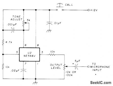
Uses NE566V PLL as tone generator, directly connected to microphone input of transmitter for activating loudspeaker in receiver being called. Operation is similar to that of paging units using selective call tones output level of PLL is adjusted so tone is same amplitude as voice.-K, Wyatt, Private Call System for VHF FM,Ham Radio, Sept,1977,p62-64 (View)
View full Circuit Diagram | Comments | Reading(766)
PHASE_CONTROLLED_D_C_SUPPLY
Published:2009/7/20 4:41:00 Author:Jessie
Uses scr's in single-phase center-tap phase-controlled rectifier. D-c voltage across load can be adjusted steplessly from zero to maximum with R7. Single ujt Q1 develops gate signal to fire both scr's on alternate half-cycles.- Silicon Controlled Rectifier Manual, Third Edition, General Electric Co., 1964, p 140. (View)
View full Circuit Diagram | Comments | Reading(1197)
_MODEL_TRAIN_THROTTLE_CONTROL
Published:2009/7/9 5:27:00 Author:May


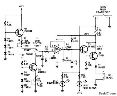
What makes this control unique is its momentum feature, which adds a degree of realism. The circuit will operate well for trains that draw up to 1 A at 15 V. None of the components are critical.In the start mode, current source Q1 charges capacitor C1. The charge current and start-up time are adjusted by resistor R2. In the stop mode, current-sink Q2 discharges capacitor C1. The discharge current and stop time are set byresistor R4. In the coast mode, op amp U1 draws very little current from C1, so the speed will remain nearly constant for some time, and then gradually decrease. Transistors Q3 and Q4 form a Darlington emitter-follower to amplify the output of U1. Diode D7 reduces the output by about 0.8 V. Another diode could be added in series to decrease the output to 0 in the stop mode. (View)
View full Circuit Diagram | Comments | Reading(1843)
MODEL_TRAIN_AND_SLOT_CAR_CONTROLLER
Published:2009/7/9 5:21:00 Author:May
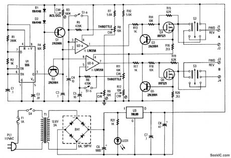
As shown, a 555 timer (U1) is configured as an astable multivibrator (oscillator) with a 400:1 duty cycle and a frequency of 40 Hz.When power is applied to the circuit, capacitor C1 (connected to pin 6 of U1) is discharged and the output of the 555 (which is used to sink current) is low. Capacitor C1 begins to charge via RI and R2 toward the positive supply rail. When the charge on C1 reaches about 66% of +V, the output of U1 at pin 3 goes high.At that point, C1 begins to discharge through R2. When the charge on C1 decreases to about 33% of the supply voltage, the output of U1 returns to the low state, and the cycle is repeated until power is removed from the circuit.When the output of U1 is low, C3 is discharged into U1 via transistor Q2. When U1 pin 3 goes high, C3 charges thr2ough a current source that consists of D1, D2, R3, R4, and Q1. The charge/discharge cycling of C3 produces a stream of pulses that are fed to the inverting inputs of U2A and U2B (an LM358 dual op amp). Two voltage-di ider networks (R7, R8, R9, and R10, R11, R12) set the reference voltage that is applied to the noninverting inputs of U1A and U1B at pins 3 and 5.Potentiometers R9 and R12 set the low-level duty cycle (5 to 10%) of U1A and U1B. They are adjusted so that the train head-lights glow, but the motor hums only slightly. Potentiometer R3 adjusts the ramp rate of C3 for 100% duty cycle at the full throttle setting. A double-pole, single-throw switch (S1A and S1B) is used to place R3/C4 and R4/C5 in the circuit.The R5/C4 and R6/C5 combinations cause the reference voltages presented to the noninverting inputs to U2A and U2B to change very slowly when the throttle is turned up and down. When the ACL/DCL switch is turned off, the resistance of the throttle-divider networks are much smaller than those of R5 and R6, so the reference voltages on C4/C5 change instantly to the new throttle setting.The output drivers consist of resistors R13 and R15, and transistors Q3 and Q4 for output A'; and resistors R17 to R20, and transistors Q5 and Q6 for output B. Components R13/R16/Q3 and R17/R20/Q5 limit the output drive currents of Q4 and Q6 to about 3 A each. Resistors R14/R15 and R18/R19 turn on Q4 and Q5, respectively, before the breakover voltage is reached to prevent damage to the output drivers and dissipate the energy that is stored in an inductive field (such as in a motor).The power supply delivers 18 V to the track. Voltage regulator U3 (a 78L09 9-V, 100-mA voltage regulator) supplies power to the control circuits.
(View)
View full Circuit Diagram | Comments | Reading(1650)
CAR_HEADLIGHT_CONTROL
Published:2009/7/9 5:01:00 Author:May
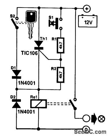
It is annoying to realize that you have left your car headlights on only to find that the battery is flat.One possible way to prevent this is with the present control.
The circuit does not provide a warning, but an action: when you switch off the ignition, relay Re1 is de-energized and the headlights are switched off-unless you deliberately decide otherwise. That decision is made possible by switch S1, which, when operated, triggers silicon-controlled rectifier Th1 so that Re1 is nergized. Notice that this is possible only when the ignition switch, S2, is off. Otherwise, the voltage across Th1 is so low, owing to shunt diode Dl, that it cannot be triggered. However, the headlights should not normally be switched on when the ignition is off; in most cases S1 will be used only rarely and the switch can then be omitted altogether. The relay should be a stan-dard 12-V car type with contacts that can switch up to 25 A. (View)
View full Circuit Diagram | Comments | Reading(1344)
SNAP_ACTION_A_C_PHASE_CONTROL
Published:2009/7/20 6:20:00 Author:Jessie
Provides snap-action switching of load in response to change in d-c signal, a-c signal, or variable resistance element, using small differentiating network R1-R2-C1 that peaks leading edge of pedestal. Triggering can occur only near beginning of each half-cycle, to give snap-on and snap-off action.- Silicon Controlled Rectifier Manual, Third Edition, General Electric Co., 1964, p 135. (View)
View full Circuit Diagram | Comments | Reading(632)
| Pages:118/312 At 20101102103104105106107108109110111112113114115116117118119120Under 20 |
Circuit Categories
power supply circuit
Amplifier Circuit
Basic Circuit
LED and Light Circuit
Sensor Circuit
Signal Processing
Electrical Equipment Circuit
Control Circuit
Remote Control Circuit
A/D-D/A Converter Circuit
Audio Circuit
Measuring and Test Circuit
Communication Circuit
Computer-Related Circuit
555 Circuit
Automotive Circuit
Repairing Circuit