
Control Circuit
Index 116
dc_MOTOR_SPEED_CONTROL
Published:2009/7/9 23:18:00 Author:May
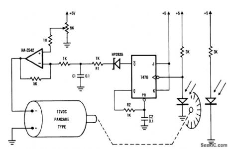
The system shown consists of the HA-2542, a small 12-Vdc motor, and a position encoder. During operation, the encoder causes a series of constant-width pulses to charge C1. The integrated pulses develop a reference voltage, which is proportional to motor speed and is applied to the inverting input of HA-2542. The noninverting input is held at a constant voltage, which represents the desired motor speed. A difference between these two inputs will send a corrected drive signal to the motor, which completes the speed control system loop.
(View)
View full Circuit Diagram | Comments | Reading(0)
TUBE_REPLACES_180°_TRANSFORMER
Published:2009/7/20 2:39:00 Author:Jessie
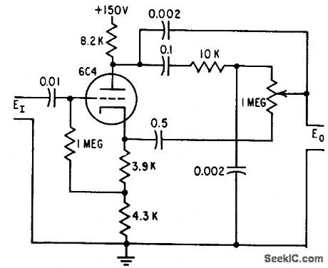
Elimination of transformer resonance effects at higher frequencies permits phase shifter to handle wider band of frequencies, from 500 to 2,000 cps for component values shown.-W. G. Shepard, Phase Shifter Range Exceeds 180°, Electronics, 31:19, p 96-100. (View)
View full Circuit Diagram | Comments | Reading(631)
PHASE_SHIFTER_WITH_LINEAR_BIASING
Published:2009/7/20 2:38:00 Author:Jessie
Frequency range of more than two decades can be obtained from voltage-controlled oscillator when linear biasing is used for phase-shift circuit.-R. A. Greiner and S. K. Morgan, Voltage Controlled Wide-Range Oscillator, Electronics, 34:51, p 31-35. (View)
View full Circuit Diagram | Comments | Reading(965)
CHILD_PROOF_RESET_SWITCH
Published:2009/7/9 23:14:00 Author:May
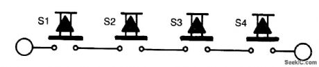
The reset switch on a computer is very important. If an operating instruction threatens to wreck the internal management of a computer, the reset button is often the only way of avoiding a possible disaster. On the other hand, it also could cause a disaster.
It is particularly important that children or pets cannot inadvertently operate the control. The circuit proposed here should put an end to your worries in this respect. Instead of one reset switch, it is necessary to press four switches simultaneously. The chances of this happening via accident, child, or pet are negligible.
The four switches are placed in positions that make it impossible to operate them all with one hand.Instead, two of them can be operated with the fingers of one hand and the other two with the fingers on the other hand. As shown, the four switches are connected in series and are intended to replace the exist-ing switch. (View)
View full Circuit Diagram | Comments | Reading(720)
LIGHT_ACTIVATED_MOTOR_DRIVE_CIRCUIT
Published:2009/7/20 2:38:00 Author:Jessie
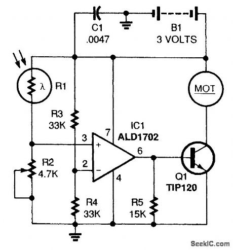
The circuit is a basic light-activated on/off switch for the motor. A CMOS op amp (IC1) is used as a voltage comparator. The comparator monitors the levels of two input voltages and switches its out-put on or off, depending on which input voltage is greater. The input on pin 2 is set to a reference voltage of about half the supply voltage by R3 and R4. The input on pin 3 is connected to a voltage divider made up of a cadmium sulfide photocell (R1) and potentiometer R2. The resistance of a photocell changes depending upon the amount of light shining on it, so the intensity of light is indicated by the voltage on pin 3 of IC1. The light level at which the circuit turns on is adjusted by R2. When the voltage on pin 3 of IC1 is greater than that on pin 2, the output (pin 6) turns on. The output of IC1 drives Q1 directly. That transistor acts like a current amplifier for the op amp. The transistor switches the motor on and off. (View)
View full Circuit Diagram | Comments | Reading(1389)
TRIP_WIRE_ALARM
Published:2009/7/9 23:13:00 Author:May
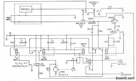
Control circuit tums converter, transmitter, and modulator on through relay contacts, to make 1,680-kc hybrid transmitter send tone-modukned signals to central station when trip wire is broken by ava lanche. Daylight on photocell initiates test transmission dcdly.-G.Neal and S. A. Stone, Hybrid Telemeter Detects Avalanches, Electtonics, 34:50, p 72-73.
(View)
View full Circuit Diagram | Comments | Reading(998)
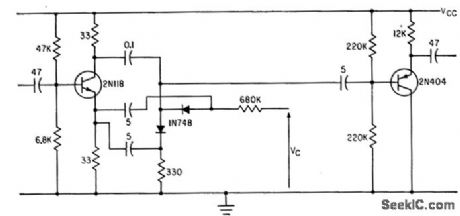
COMPRESSOR_PROTECTOR
Published:2009/7/9 23:13:00 Author:May
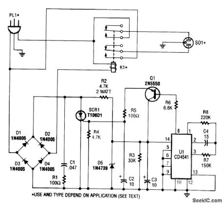
This circuit monitors the power-line (ac) voltage.When a power failure occurs,on restoration of power,the circuit adds a five-minute delay before energizing K1,which protects the compressor against limited low voltage.
U1 is a 16-stage counter with an integral oscillator that is set to divide by 8192. R7, R8, and C4 set the oscillator frequency to about 25 Hz, which produces a total count interval of 300 seconds (5Mnutes). After this time, pin 8 U1 goes high, which forward biases Q1,triggers SCR1,and activates K1. Up to 30 A can be switched.
(View)
View full Circuit Diagram | Comments | Reading(1870)
PM_DC_MOTOR_SPEED_CONTROL_
Published:2009/7/20 2:37:00 Author:Jessie
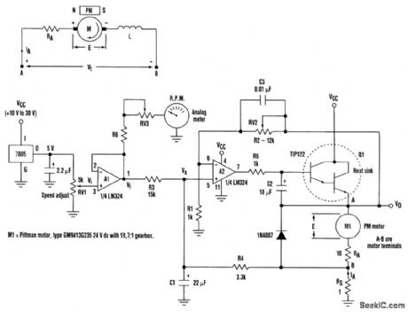
Speed control of permanent-magnet (PM) dc motors with the aid of optical or dc tachometers is generally inconvenient and difficult, particularly on motors with integral gearboxes. The high-speed shaft of the motor that drives the gearbox isn't always accessible and the speed of the geared-down shaft often is too low for tachometers. Described here is a single-supply regulating speed-control circuit that doesn't require a tachometer. It keeps the motor torque high under load by using positive feedback to compensate for the drop caused by armature resistance. In unregulated variable-speed PM dc motor systems, the drop in speed under load is particularly pronounced at low motor-supply voltages. The positive feedback generates a negative resistance that compensates for the nonlinear effects caused by armature resistance. It thereby ensures that the speed-control input voltage (Vi) linearly controls the speed of the motor. Armature resistance compensation is achieved if:
RS= RA/[gain(R3) / (R3 + R4)] - 1
The divider action of R3 and R4 together with the gain reduces the value required for Rs to minimize the power dissipation. C1 and R4 dampen the positive-feedback signal's response time, but they also form a low-pass filter and attenuate the motor current noise fed to the A2 input. The maximum output voltage swing from A2 is approximately VCC-2 V, and there is a 1.2-V Vbe loss by T1. This implies that the supply voltage (Vcc) should be about 5 V above the maximum desired motor voltage in order to allow for extra output drive to the motor under heavy load conditions. A reason-able choice for Rs is approximately RA/10, and the gain of A2 should be trimmed with RV2 to ensure that the motor's speed does not drop when loaded. (View)
View full Circuit Diagram | Comments | Reading(4467)
PRINTER_ERROR_ALARM
Published:2009/7/9 23:12:00 Author:May
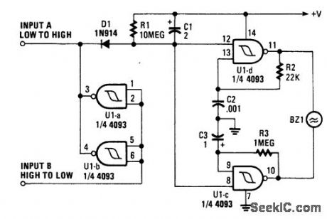
When a printer is shut down, this alarm sounds an alarm. The input can be either a high-to-low or low-to-high transition. This can be a logic level that corresponds with the printer being on or off. The oscillator produces an interrupted (on-off) tone. (View)
View full Circuit Diagram | Comments | Reading(871)
SWITCH_DEBOUNCER_WITH_AUTO_REPEAT
Published:2009/7/9 23:11:00 Author:May
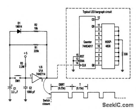
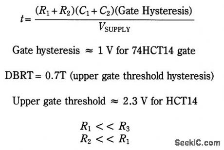
This circuit produces an output pulse when SW1 (pushbutton) is depressed. It also becomes a hysteresis gate oscillator. D1 and R2 add asymmetry. The DBRT (delay before repeat time) is caused by the oscillator start-up conditions: C1 has to change from zero to the upper gate threshold rather than to the lower threshold.
The auto repeat time:
(View)
View full Circuit Diagram | Comments | Reading(944)
LIGHT_CONTROLLER
Published:2009/7/9 23:09:00 Author:May
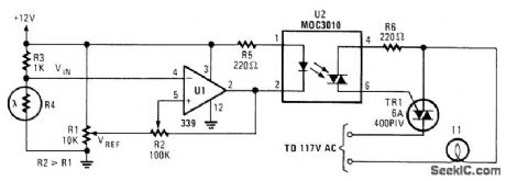
A photocell drives U1, acomparator, which controls optocoupler U2. A 6A Triac is used to switch an ac load,such a lamp,etc. (View)
View full Circuit Diagram | Comments | Reading(850)
INTRUDER_ALARM
Published:2009/7/9 23:08:00 Author:May
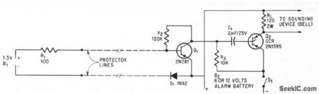
Circuit responds to break or short in loop of foil or wire encircling area to be protected, by reacting to change in normal current droin of 500 microamp from l.5.v battery in protector loop. Circuit is reset after alarm by opening SI1 momentarily,-W. Vollenweidel,Low-Current Alarm,Electronics,39:5,p 105-106.
(View)
View full Circuit Diagram | Comments | Reading(0)
360_DEG_SHIFTER
Published:2009/7/20 2:42:00 Author:Jessie
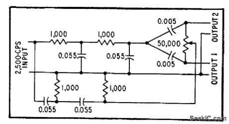
One variable component provides phase difference between outputs that is adjustable from -180 to +180 degrees without substantial change in magnitude, at fixed frequency of 2,500 cps,-W. Bacon, Circuit Shifts Phase 360 Degrees, Electronics, 31:23, p 94-97. (View)
View full Circuit Diagram | Comments | Reading(595)
MEASURING_PHASE_UP_TO_400_MC
Published:2009/7/20 2:41:00 Author:Jessie
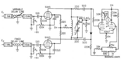
Three plug-in tuning circuits cover range from 15 to 400 Mc. Phase delay is compared with continuously variable delay standard with accuracy of 1% or 0.1°.-Y. P. Yu, How to Measure Phase at High Frequencies, Electronics, 34:11, p 54-56. (View)
View full Circuit Diagram | Comments | Reading(625)
TONE_DECODER
Published:2009/7/20 1:57:00 Author:Jessie
Replaces resonant reeds commonly used in multichannel radio-con-trolled models to detect modulation frequency being transmitted. Use of IC logic has advantage that range of audio frequencies can exceed an octave, whereas reeds cannot because they respond to second harmonic. Decoder has digital high-pass characteristic that is passed through inverter to give digital low-pass characteristic. Values of RX, and CX determine critical frequency; for 900 Hz, use 150,000 ohms and 0.015 μF. To obtain n nonoverlapping bandpass characteristics, n - 1 basic elements with different critical frequencies are required; components to left of dashed line may be common to all these elements. Article covers multichannel systems in detail, along with use of time-division multiplexing.-C. Attenborough, Radio Control Tone Decoder, Wireless World, Dec.1973, p 593-594. (View)
View full Circuit Diagram | Comments | Reading(2389)
3_WAY_LIGHT_CONTROL
Published:2009/7/9 23:04:00 Author:May

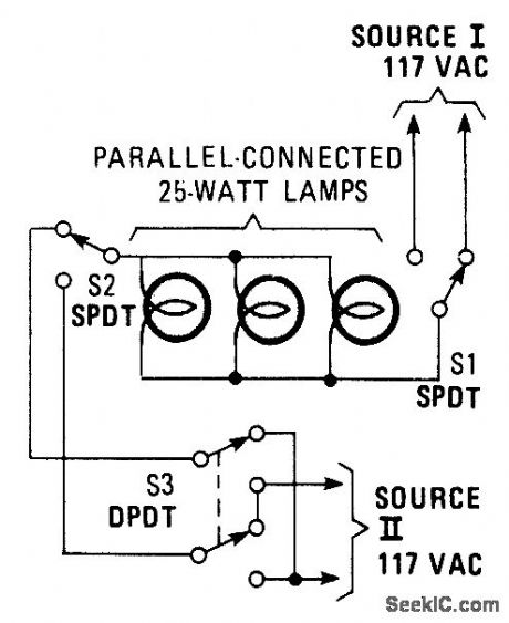
This hookup is useful in some house wiring situations, where only two wires are available between switches,rather than the 3-way setup where 3 wires are requires.S1 and S2 are ordinary three-way switches and S3,a DPDT switch,is commonly avaliable as a four-way switch at hardware stores. (View)
View full Circuit Diagram | Comments | Reading(735)
TWO_TONE_CONTROL
Published:2009/7/20 1:55:00 Author:Jessie
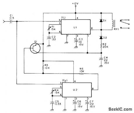
Used to perform simple ON/OFF auxiliary function via repeater input,Two 567 decoders energize relay for input tone of 1800Hz,with latching, and release it for 1950Hz Diodes are 1N4001,Relay can be 12 or24 V,al is 2N3905,2N3906,MPS6521,or 2N2222.-W Hosking. A Single Tone Can Do It,73Magazine, Nov 1977,p184-185 (View)
View full Circuit Diagram | Comments | Reading(768)
500_Hz_CONTROL_TONE
Published:2009/7/20 1:53:00 Author:Jessie
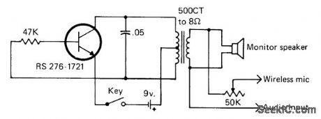
Developed for use as wireless FM remote control for keying transmitter at another location by sending keyed audio tone over radio link, acoustic link fed by loudspeaker, or audio line. Frequency is about 500 Hz.-J. Schultz, H.F, Operating-Remote Control Style, CQ, March 1978, p 22-23 and 90. (View)
View full Circuit Diagram | Comments | Reading(611)
PLL_TONE_DECODER
Published:2009/7/20 1:52:00 Author:Jessie
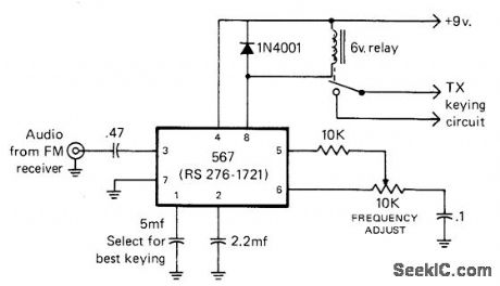
Used in simple wireless FM remote control set up for keying transmit-ter. Keyed 500-Hz tone output of FM receiver at transmitter site acts through 567 PLL to operate 6-V relay whose contacts are in keying circuit of transmitter.-J. Schultz, H.F. Operating-Re mote Control Style, CQ, March 1978, p 22-23 and 90. (View)
View full Circuit Diagram | Comments | Reading(1435)
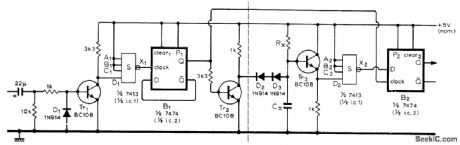
BLIP_AND_HOLD_RADIO_CONTROL
Published:2009/7/20 1:50:00 Author:Jessie
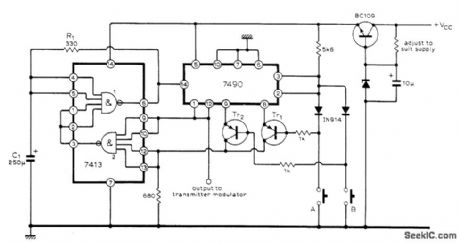
Coder uses two ICs to generate sequence of pulses suitable for actuators of radio control system. During standby, oscillator formed by NAND gate 1 operates at 0.5 Hz as determined by C1 and R1, and all four outputs of 7490 IC are zero. When switch AL is closed, 7490 is clocked by negative edge of oscillator waveform and Tr1 becomes forward-biased. Output of NAND gate 2 then drops to zero, stopping oscillator and holding outputs of 7490. When switch A is opened, outputs of 7490 again drop to zero. Many different blip-and-hold combinations can be obtained by suitable arrangement of switches and gates.-G. D. Southern, Sequence Generator for Radio Control, Wireless World, Jan. 1976, p 60. (View)
View full Circuit Diagram | Comments | Reading(889)
| Pages:116/312 At 20101102103104105106107108109110111112113114115116117118119120Under 20 |
Circuit Categories
power supply circuit
Amplifier Circuit
Basic Circuit
LED and Light Circuit
Sensor Circuit
Signal Processing
Electrical Equipment Circuit
Control Circuit
Remote Control Circuit
A/D-D/A Converter Circuit
Audio Circuit
Measuring and Test Circuit
Communication Circuit
Computer-Related Circuit
555 Circuit
Automotive Circuit
Repairing Circuit