
Control Circuit
Index 102
70_MC_NEUTRALIZED_GAIN_CONTROLLED_AMPLIFIER
Published:2009/7/16 2:18:00 Author:Jessie
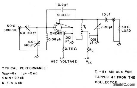
Gain is 27 db, with typical noise figure below 3 db. RC for reverse gain control is 0 ohms, and for forward gain control is 1,000 ohms. Reverse control range is 35 db, and forward gain control is 47 db.-Texas Instruments Inc., Solid-State Communications, McGraw-Hill, N.Y., 1966, p 215. (View)
View full Circuit Diagram | Comments | Reading(779)
VOLTAGE_CONTROLLED_GAIN
Published:2009/7/16 2:17:00 Author:Jessie
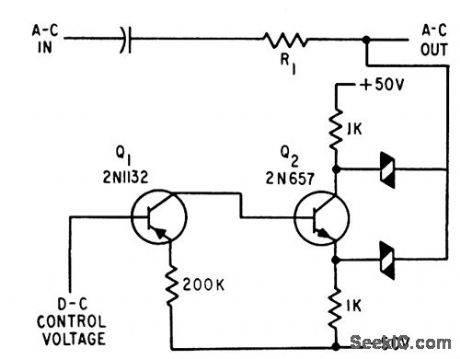
Response of two-transistor a-c amplifier, controlled by d-c voltage, can be mode linear by adding suitable feedback. With no d-c control voltage on base of Q1, both transistors are saturated, and effective shunt resistance of circuit is about 500,000 ohms, When d-c control voltage is increased positively until Q1 is cut off, effective shunt resistance drops to 200,000 ohms.-L. C. Bowers, Attenuator Controls Amplifier Gain, Electronics, 34:39, p 150-153. (View)
View full Circuit Diagram | Comments | Reading(0)
CASCADED_AGC
Published:2009/7/16 2:15:00 Author:Jessie
Double-conversion i-f uses two separate agc amplifiers to get good temperature stability and low noise figure with transistor amplifiers.-J. S. Brown, Improving Gain Control of Transistor Amplifiers, Electronics, 34:17, p 108-110. (View)
View full Circuit Diagram | Comments | Reading(904)
AMPLIFIED_AGC_1
Published:2009/7/16 2:10:00 Author:Jessie
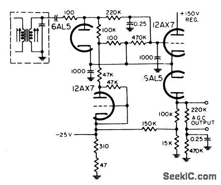
Uses d-c amplifier in agc circuit to keep output of communication receiver more nearly constant despite widely varying input signal. One drawback of amplified agc is that when d-c ampliler plate current drops, bias voltage at its cathode increases agc output and thereby reduces gain of controlled stages.-NBS, Handbook Preferred Circuits Navy Aeronautical Electronic Equipment, Vol. 1, Electron Tube Circuits, 1963, p N 12-4. (View)
View full Circuit Diagram | Comments | Reading(815)
AMPLIFIED_AGC
Published:2009/7/16 2:08:00 Author:Jessie
Uses d-c amplifier in agc circuit to keep output of communication receiver more nearly constant despite widely varying input signal.-NBS, Handbook Preferred Circuits Navy Aeronautical Electronic Equipment, Vol. 1, Electron Tube Circuits, 1963, p N 12-4. (View)
View full Circuit Diagram | Comments | Reading(962)
THYRISTOR_SWITCH
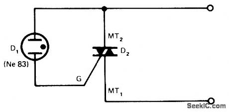
Published:2009/7/13 20:52:00 Author:May
When circuit of conventional P-gate thyristor is grounded by switch, negative-going pulse is applied to thyristor cathode, which reverse-biases the diode. When thyristor conducts, diode is forward-biased and has only about 0.7-V drop. Use low-voltage diode, rated for full load current. Opening of relay contacts makes circuit switch off.-R. V. Hartopp, Grounded Gate Thyristor, Wireless World, Feb. 1977, p 45.
(View)
View full Circuit Diagram | Comments | Reading(1206)
VOLTAGE_SENSITIVE_SWITCH
Published:2009/7/13 20:42:00 Author:May
RCA 40527 triac is triggered by small neon. After breakdown occurs bidirectionally at 88 V, triac takes over as short-circuit. D1 can be any other voltage breakdown device, such as diac or zener, and thyristor can be used in place of triac to give unilateral switching. Applications include use as power crowbar, with breakdown level set by artificial resistance-controlled zener.-L. A. Rosenthal, Breakdown and Power Devices Form Unusual Power Switch, EDN Magazine, July 5, 1974,p74-75. (View)
View full Circuit Diagram | Comments | Reading(1080)
PERFECT_AC_SWITCH
Published:2009/7/13 20:39:00 Author:May
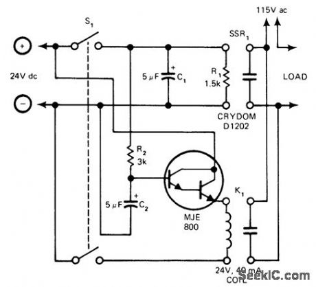
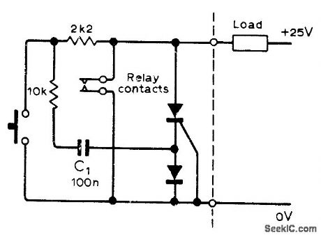
Developed for use in computdrized equipment to prevent generation of severe noise spikes if contact closure can occur at any point in AC cycle. Closing S1 gates solid-state relay SSR1, which noiselessly switches load at next zero crossing. During this time, C2 charges through R2, After time T = 3R2C2, MJE800 Darlington is turned on, pulling in relay K1 to follow up SSR1 with hard contacts.When S1 is later opened, K1 drops out immediately but C1 discharges through gate of SSR1 to hold it on for about T = 6R1C1. Load is then switched off at next zero crossing after this delay.-E. Woodward, This Circuit Switches AC Loads the Clean Way, EDN Magazine, Nov. 20, 1975, p 160 and 162. (View)
View full Circuit Diagram | Comments | Reading(855)
AUTODYNE_CONVERTER
Published:2009/7/13 20:23:00 Author:May
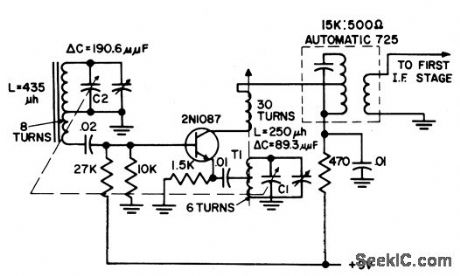
Single transistor stage serves as combination local oscillator, mixer, and i-f amplifier in transistor radio.Mixer operates in grounded-emitter configuration. I-f value is 455 kc.- Transistor Manual, Seventh Edition, General Electric Co.1964, p284. (View)
View full Circuit Diagram | Comments | Reading(1908)
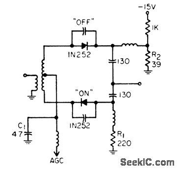
DOUBLE_GATED_AGC
Published:2009/7/16 3:00:00 Author:Jessie
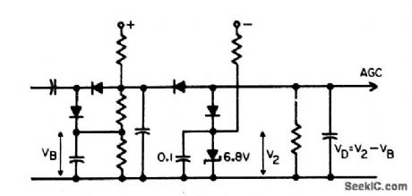
Uses zener diode to supply standing bias for agc bus. -W. A Rheinfelder, Designing Automatic Gain Control Systems, EEE, 13;1, p 53-57. (View)
View full Circuit Diagram | Comments | Reading(635)
DIODE_T_ATIENUATOR_AGC
Published:2009/7/16 2:59:00 Author:Jessie
All three diodes are simultaneously controlled, to give excellent agc action over control range of 20 db, although insertion loss is high. Frequency response is excellent up to 150-Mc cutoff.-W.A. Rheinfelder, Designing Automatic Gain Control Systems, EEE, 13:1, p 53-57. (View)
View full Circuit Diagram | Comments | Reading(670)
NINE_FIXED_GAIN_STAGES_GIVE_AGC
Published:2009/7/16 2:58:00 Author:Jessie
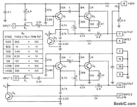
Monopulse radar amplifier stages are used in cascade, each with different fixed gain and a slicer that switches from that gain to unity gain if signal exceeds predetermined reference level. Give gain up to 80 db in 0.5-db steps, equivalent to fast agc, to give constant 10-v output for signals ranging from 1 mv to 10 mv. -W. W. Smith, Fast AGC Amplifier Locks Monopulse Radar on Target, Electronics, 36:39, p 34-36. (View)
View full Circuit Diagram | Comments | Reading(726)
SIMPLE_AGC
Published:2009/7/16 2:57:00 Author:Jessie
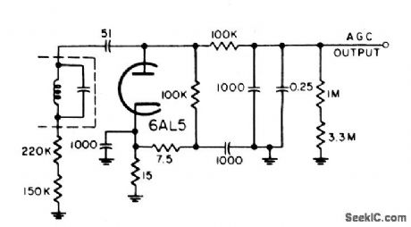
Used to keep output of communication receiver relatively constant with varying input signals.-NBS, Handbook Preferred Circuits Navy Aeronautical Electronic Equipment, Vol. 1, Electron Tube Circuits, 1963, p N 12-4. (View)
View full Circuit Diagram | Comments | Reading(1013)
AGC_WITH_VARICAP_DIODE_BRIDGE
Published:2009/7/16 2:56:00 Author:Jessie
Uses voltage-controlled capacitors to provide very large gain control range, greater than 30 db.-W. A. Rheinfelder, Designing Automatic Gain Control Systems, EEE, 13:1, p 53-57. (View)
View full Circuit Diagram | Comments | Reading(768)
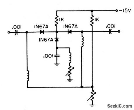
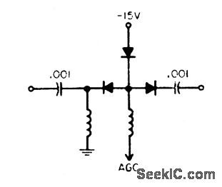
DIODE_L_ATTENUATOR_AGC
Published:2009/7/16 2:55:00 Author:Jessie
Two diodes provide maximum agc control. Circuit gives control range of about 15 db with agc voltages to 3 v. Above 200 Mc, frequency response changes irregularly with attenuation.-W. A. Rheinfelder, Designing Automatic Gain Control Systems, EEE, 13:1, p 53-57. (View)
View full Circuit Diagram | Comments | Reading(791)
AGC_FOR_ADF
Published:2009/7/16 2:54:00 Author:Jessie
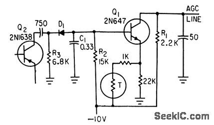
Gives uniform receiver response over wide dynamic range of input signal levels. Output of third i-f stage Q2 is applied across agc diode D1.-P. V. Sparks, Servo Filter and Gain Control Improve Automatic Direction Finder, Electronics,34:23, p 110-113. (View)
View full Circuit Diagram | Comments | Reading(742)
AGC_WITH_VARICAP
Published:2009/7/16 2:53:00 Author:Jessie


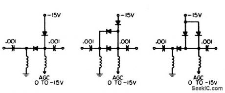
Basic voltage-controlled capacitor circuit uses capacitance variation with voltage of back-biased diode constructed to have large capacitance changes, such as Varicap. Circuits give different insertion losses and gain changes. Left: 5 db insertion loss and 16 db gain control range for agc bias of 15 v. Center: 2 db loss and 11 db gain range. Right: 7 db loss and 18 db gain range. AII can be reasonably flat for 200-Mc bandwidth.-W. A. Rheinfelder, Designing Automatic Gain Control Systems, EEE, 13;1, p 53-57. (View)
View full Circuit Diagram | Comments | Reading(855)
200_MC_GAIN_CONTROLLED_STAGE
Published:2009/7/16 2:51:00 Author:Jessie
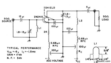
Has gain of 17 db With typical noise figure of 3 db,24 db of forward gain control,and 33 db of reverse gain contral.-Texas Instruments Inc., solid-State Communications, McGraw-Hill, N,Y., 1966,p 218. (View)
View full Circuit Diagram | Comments | Reading(670)
BRIDGE_WITH_AGC_ON_BOTH_DIODES
Published:2009/7/16 2:50:00 Author:Jessie
Agc is applied to center tap of transformer, to turn one diode off while other is being turned on. Attenuation can be 40 db over bandwidth up to 250 Mc with agc bias of 0.5 to 3 v. Insertion loss is only a few db.-W.A. Rheinfelder, Designing Automatic Gain Control Systems, EEE, 13:1, p 53-57. (View)
View full Circuit Diagram | Comments | Reading(778)
AGC_WITH_DIODE_T_NETWORK_VARICAP
Published:2009/7/16 2:48:00 Author:Jessie
Voltage-controlled capacitor circuit minimizes effect of shunt capacitance, thus reducing resonance peaks and preventing regeneration, but insertion loss is high (8 db).-W. A. Rheinfelder, Designing Automatic Gain Control Systems, EEE, 13:1, p 53-57. (View)
View full Circuit Diagram | Comments | Reading(746)
| Pages:102/312 At 20101102103104105106107108109110111112113114115116117118119120Under 20 |
Circuit Categories
power supply circuit
Amplifier Circuit
Basic Circuit
LED and Light Circuit
Sensor Circuit
Signal Processing
Electrical Equipment Circuit
Control Circuit
Remote Control Circuit
A/D-D/A Converter Circuit
Audio Circuit
Measuring and Test Circuit
Communication Circuit
Computer-Related Circuit
555 Circuit
Automotive Circuit
Repairing Circuit