
Control Circuit
Index 120
SMALLEST_PHASE_CONTROL
Published:2009/7/20 6:32:00 Author:Jessie
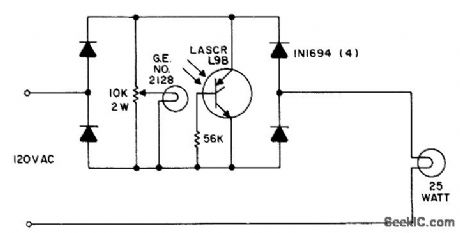
Miniature lamp No. 2128 with small, low-mass filament can reach firing level of light-activated scr in about three cycles with low applied voltage. As applied voltage is increased, this time is reduced to about 1 millisec when lamp is directed across LASCR terminals, thus providing phase control. Lamp voltage is removed when LASCR fires, protecting lamp and resetting it for next half-cycle. Useful for dimming 25-w lamp or for controlling temperature of small soldering iron.- Silicon Controlled Rectifier Manual, Third Edition, General Electric Co., 1964, p 213. (View)
View full Circuit Diagram | Comments | Reading(837)
HIGH_GAIN_PHASE_CONTROL
Published:2009/7/20 6:25:00 Author:Jessie

Use of two different sizes of charging capacitors in series increases effective gain up to 10,000 times that of conventional ujt/scr phase-control circuit. Eliminates amplification.- Transistor Manual, Seventh Edition, General Electric Co., 1964, p 332. (View)
View full Circuit Diagram | Comments | Reading(828)
WATER_LEAK_ALARM
Published:2009/7/9 3:12:00 Author:May
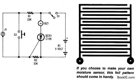
A sensor connected to J1 causes SCR1 to conduct, which sounds buzzer BZ1. The sensor is a PC-board foil pattern grid. Several sensors can be wired in parallel for increased coverage or to monitor sev-eral places simultaneously. (View)
View full Circuit Diagram | Comments | Reading(959)
HIGH_PERFORMANCE_VIDEO_SWITCH
Published:2009/7/9 3:09:00 Author:May

This figure shows a one-of-two switch with a summing amplifier. The video source's line can be termi-nated either externally or internally to switch R0. With this termination resistor, a load change of less than 1 Ω will be seen by the source when the switch changes state. For this reason, input isolation amplifiers are not necessary. R4 can be varied to control circuit gain, but should never be less than 1400 Ω since the NE5539 is internally compensated for gain values greater than seven. A value of approximately 2500 Ω for R4 will set circuit gain to near unity. Additionally, the circuit output impedance is set by R6, and R5 sets the output dc offset to near zero. (View)
View full Circuit Diagram | Comments | Reading(868)
AUTOMATIC_VIDEO_SWlTCH
Published:2009/7/9 3:06:00 Author:May
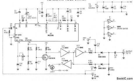
Turn on a game, computer, videodisc player, or whatever, and its output takes priority over the antenna-derived signal-the antenna is disconnected and the alternate source is fed to the monitor. When the alternate video source is no longer detected, the switch automatically reconnects the antenna. When the rf carrier is detected, a high logic output appears at pin 15 of U1-squelch status. The signal is then buffered to VMOS FET Q1. This FET can drive CMOS inverter/buffer U2, can be an open-drain output to drive a relay, or can convert to a 5 V logic level. When pin 15 of U1 becomes high, Q1 turns on, pulling pin 11 of U2e low; in turn, pin 12 becomes high. The output of U2e is fed to U2f, forcing its output, at pin 15, low. When the signal at U2 pin 12 is high, D1 is biased on, allowing the signal at J3 to flow through C14, D1, and out to J2 through C13. When the signal at J3 is removed, U1 pin 15 decreases. That decrease causes U2 pin 12 to decrease and U2 pin 15 to increase. When the signal at U2 pin 15 is high, it biases D2 on, allowing the signals at J1 to flow through C12, D2, and out to J2 through C13. (View)
View full Circuit Diagram | Comments | Reading(1270)
RAIN_ALARM
Published:2009/7/9 3:00:00 Author:May
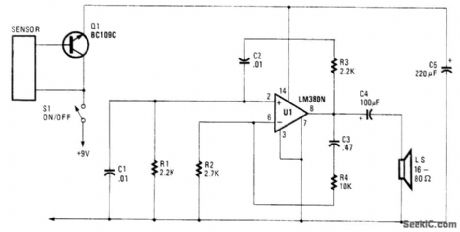
This rain sensor causes Q1 to conduct when conductive liquid (rainwater, etc.) applies bias to its base.This bias triggers LM380N oscillator and causes LS to emit a tone. (View)
View full Circuit Diagram | Comments | Reading(0)
VIDEO_SIGNAL_CLAMP
Published:2009/7/9 2:59:00 Author:May
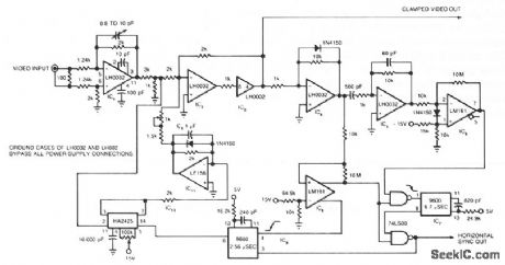
The circuit uses a track-and-hold amplifier in a closed-loop configuration to clamp the back-porch voltage of a standard video waveform to O V. The circuit's outputs include a clamped composite-video signal and a TTL-level horizontal-blanking pulse. Differential input buffer IC1 and the summing amplifier IC2 isolate the input video signal. Clipper IC4 removes the video signal, leaving only the synchronization information. Differentiator IC5 detects the edges of the horizontal blanking pulses and produces pulses that correspond to the leading and trailing edges of the horizontal blanking pulses. IC6 clips these pulses and converts them to a TTL level. IC7 uses these clipped pulses to generate a TTL-level window that, when combined with the horizontal pulse generated by IC8, forms a TTL representation of the original horizontal pulse. This representation is synchronized to the input waveform. IC9 uses the trailing edge of this reconstructed waveform to generate the track pulse for track-and-hold amplifier IC10. IC11 filters 1010's dc output and, after gain adjustment, feeds it back to IC2's summing node. (View)
View full Circuit Diagram | Comments | Reading(1744)
FLOOD_ALARM
Published:2009/7/9 2:57:00 Author:May


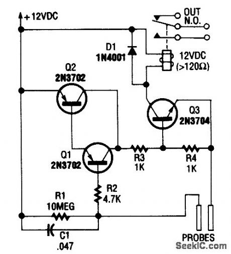
Using a few bipolar transistors, this circuit acts as a flood alarm. When liquid touches the probes,leakage current biases Q1, Q2, and Q3 (a dc-cou pled amplifier) into conduction, which activates the relay. The contacts can be hooked into the alarm system. (View)
View full Circuit Diagram | Comments | Reading(0)
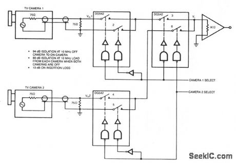
GENERAL_PURPOSE_VIDEO_SWITCH
Published:2009/7/9 2:54:00 Author:May
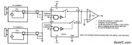
The circuit shown provides 40-dB isolation at 6 MHz and is good for general purpose video switching. (View)
View full Circuit Diagram | Comments | Reading(0)
The auto control circuit of the stone pile hammer
Published:2011/7/22 6:37:00 Author:qqtang | Keyword: auto control circuit, pile hammer

The working principle of the circuit The auto control circuit of the stone pile hammer consists of the power supply circuit, current detection and indicating circuit and the control alarm circuit, see as figure 8-141.
The power supply circuit consists of the transformer T, rectifier bridge pile UR, filter capacitors C2 and C3 and the 3-phase regulated integrated circuit IC2. The current detection and indicating circuit consists of the mutual inductor TAl-TA3, resistor R1-R4, potentiometer RP1, diode VD1, capacitor C1, ampere meters of PA1 of PA2 and computer integrated circuit IC1. (View)
View full Circuit Diagram | Comments | Reading(778)
The plastic regenerator control circuit
Published:2011/7/21 22:21:00 Author:qqtang | Keyword: plastic regenerator, control circuit
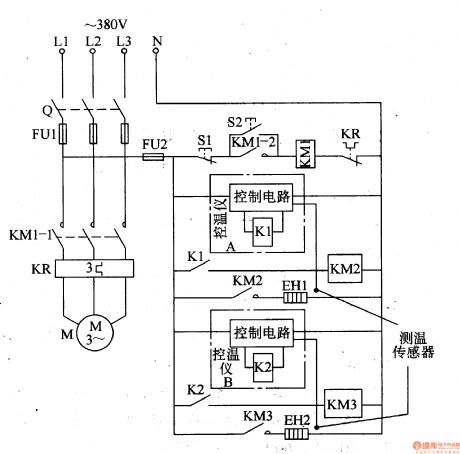
The working principle of the circuit The plastic regenerator control circuit consists of the motor main control circuit and electric heater temperature control circuit, see as figure 8-140.
The motor main control circuit consists of edge switch Q, fuses of FU1 and FU2, the AC contactor KMI, heat relay KR, stop key SI, starting key S2 and motor M. The heater temperature control circuit consists of the AC contactors of KM1 and KM2, the temperature controllers A and B, the plastic pre-heater EHI and melting heater EH2. (View)
View full Circuit Diagram | Comments | Reading(762)
WATER_LEVEL_CONTROL
Published:2009/7/9 2:28:00 Author:May
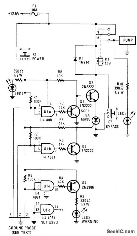
This circuit will power up a water pump when the water reaches a predetermined level. Then it turns itself off when the water recedes to another predetermined point.
Gates U1A through U1C each have their two inputs tied together, and serve as probes. The probes are then placed at various levels to trigger a particular function at a predetermined time. The ground side of the circuit is placed below the mini-mum water level. The inputs to each gate are tied high through a 100-kΩ resistor connected to the +12.5-V bus.
As the water level slowly rises to probe L, the input to U1A is pulled low by the conduction of current through the water to the ground probe. That turns Q1 off and Q2 on. With Q2 turned on, the ctr-cuit is placed in the standby mode, ready to activate the pump when conditions are right.
Probe 2 is placed at the maximum water level.If the water level reaches probe 2, the input of U1B is brought low, turning Q3 on, which, in tum, causes current to be applied to the gate of SCR1, turning it on. The circuit through K1, Q2, and SCR1 is now complete to ground, and the water pump is now turned on, which causes the water level to recede. When the water level falls below probe 2, U1B goes back to logic high.
However, because of the latching nature of SCR1, the pump continues to run until the water level falls below probe 1. At that point, the ground circuit opens and de-energizes K1, which turns the pump off. The pump will not tum on again until the water level again rises above probe 2.
Probe 3 was added as a warning. If the water level reaches probe 3, LED2 indicates that the pump is not working. Switch S2 is a manual over-ride and S1 powers the sensing circuit. LED3 indi-cates that power has been applied to the pump.LED1 indicates that power has been applied to the sensor. (View)
View full Circuit Diagram | Comments | Reading(0)
VIDEO_SWITCH_WITH_VERY_HIGH_OFF_ISOLATION
Published:2009/7/9 2:22:00 Author:May
View full Circuit Diagram | Comments | Reading(703)
FLASHINGLED_CONTROLLER
Published:2009/7/9 2:18:00 Author:May
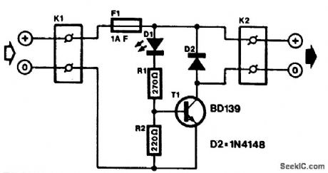
The LED with integrated flasher is connected in series with the base-emitter junction of transistor T1. Thus, the load connected to K2 is switched on and off in rhythm with the flash rate. This load can be a relay or a lamp.
The maximum collector current of the transistor (of the BD139=750mA) must not be exceeded. If that is not sufficient, a power Darlington can be used, which will give some amperes. The current drawn by the circuit under no-load conditions amounts to 20mA. (View)
View full Circuit Diagram | Comments | Reading(1040)
Home booster pump protection circuit diagram
Published:2011/8/2 2:37:00 Author:Rebekka | Keyword: Home booster pump protection
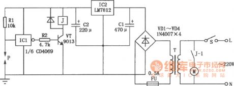
The power supply switch S will be closed if the water pipe has not water, P and the ground is similar to insulation condition, the inverter ICl inputs high, outputs low, VT cuts off, J is released. Its tragger J-1 cuts off, M booster pump is not running avoiding pump idling. If the pipe has water, P and steel shell pass the water and resistance will be conducted, then ICl input is low level and output is high level, VT will be conducted, J pulls in, M operates normally. IC1 uses CD4069 six-inverter, the one shown in the figure only uses one group of inverters, and the rest 5 groups of inverters is vacant(Connect all the input ends to the ground to prevent interference.) P is the detection sensor when there is not water, you need to make it by yourself. Methods: Drill a hole in the pipe, spark plugs into the car, pay attention to the pad to prevent leakage, eads to P pole at the spark needle, water pipe(steel) chassis can connect to the ground. (View)
View full Circuit Diagram | Comments | Reading(1327)
STROBE_ALARM
Published:2009/7/9 1:55:00 Author:May
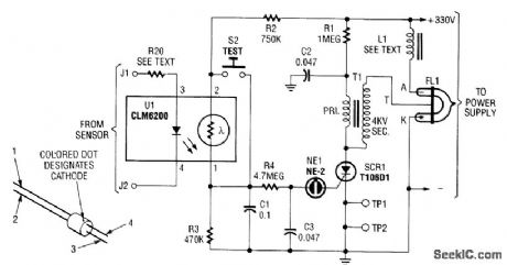
This strobe gives a visual indication of a sensor input. The input signal causes U1, a light dependent resistor, to charge C1 and C3 through R4. When NE1 fires, C3 discharges into SCR1, which triggers it and causes C2 to discharge through trigger transformer T1, which triggers Flashlamp FL1. The 330-V supply should have about 50 to 100 μF output capacitance. L1 supplies about 25-mH inductance to prolong the flash and the life of FL1. (View)
View full Circuit Diagram | Comments | Reading(1383)
PEAK_PICTURE_CONTROL
Published:2009/7/20 20:43:00 Author:Jessie
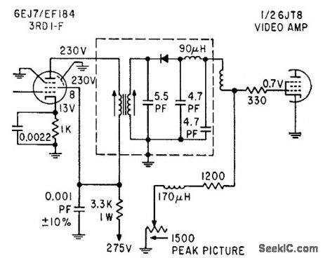
Variable resistor in video detector load circuit can be adjusted to improve snowy pictures in fringe areas.-Tv Set Size Shrinks, Electronics, 36:23, p 22.
(View)
View full Circuit Diagram | Comments | Reading(872)
9V 55mA AC and DC converter circuit composed of TNY253P
Published:2011/8/3 2:39:00 Author:Rebekka | Keyword: 9V , 55mA , AC and DC , converter

9V 55mA AC and DC converter circuit composed of TNY253P is shown as above. It can enable the end (EN) hang in air to simplify the circuit, TNY253P operates in the continuous conducting mode and outputs constant power. The output voltage is set by the regulator VDz. (View)
View full Circuit Diagram | Comments | Reading(712)
Current three-phase motor phase-failure protection circuit diagram
Published:2011/8/2 2:39:00 Author:Rebekka | Keyword: Current three-phase motor, phase-failure protection
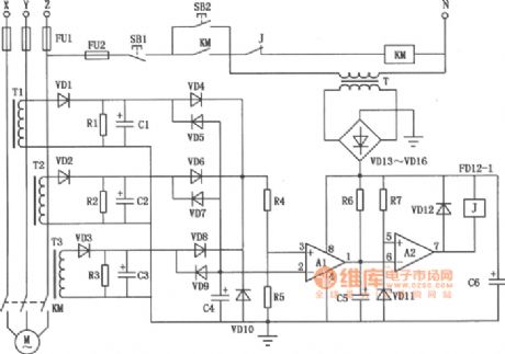
The production of transformer Tl ~ T3 can use the ring ferrite core which is easy to be purchased on the market. It uses Φ0.25mm high-strength wire wound with 150 to 250 turns. The number of the turns is determined by the motor power. If the motor power is low, you can wound more turns. The power supply line passes the ring. The capacitors C1 ~ C3 use the 10μF/25V electrolytic capacitors. C4 uses 0.1μF/63V ceramic chip capacitor; C6 uses 470μF/25V electrolytic capacitor; C5 is the interference absorption capacitor, when the action is too sensitive, it can increase the capacitance value of C5, conversely it will reduce the value of C5, its range is 4.7 ~ 33μF/25V. Resistors Rl = R2 = l.2kΩ, R4 = 390kΩ, R5 = 680kΩ, R6 = 15kΩ, R7 = 2kΩ, the nominal power resistor is 1/8W RJ. Zener VD11's regulator value is about 8V. Other diodes use 1N4004. (View)
View full Circuit Diagram | Comments | Reading(4339)
UP_DOWN_RAMP_CONTROL
Published:2009/7/20 23:10:00 Author:Jessie
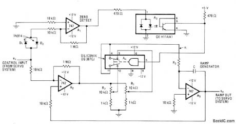


Siliconix DG387CJ solid-state relay A4 provides switch-ing from up ramp to down ramp for decelerating servo when it zeroes in on correct new position. Slopes are determined by settings of R1 and R2. Arrangement ensures optimum senro system response at low cost. A1 detects that input is other than 0 V and energizes optoisolator A3 for switching A4. Resulting positive-going ramp from A5 moves system load toward desired position, making feedback voltage of servo reduce control-input voltage. When this drops to within 0.7 V of ground, A1 goes low and A3 turns off. A4 now initiates down-ramp waveform to decelerate system to stop. For ramp rate of 20V/s, C can be 0.33μF and R3 1.8 megohms.-R.E. Kelly, Up-Down Ramp Quickens Servo System Response, Electronics, July 20, 1978, p 121 and 123. (View)
View full Circuit Diagram | Comments | Reading(1126)
| Pages:120/312 At 20101102103104105106107108109110111112113114115116117118119120Under 20 |
Circuit Categories
power supply circuit
Amplifier Circuit
Basic Circuit
LED and Light Circuit
Sensor Circuit
Signal Processing
Electrical Equipment Circuit
Control Circuit
Remote Control Circuit
A/D-D/A Converter Circuit
Audio Circuit
Measuring and Test Circuit
Communication Circuit
Computer-Related Circuit
555 Circuit
Automotive Circuit
Repairing Circuit