
Control Circuit
Index 108
HELMET_LAMP_DIMMER
Published:2009/7/12 22:43:00 Author:May
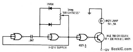
Provides lossless variation in brightness of incandescent lamp by using duty-cycle modulation. All three sections of 4025 triple three-input NOR gate turn lamp on and off rapidly at rate determined by setting of brightness control pot in astable MVBR circuit, Output transistor rating must be sufficient to handle lamp current.-D. Lancaster, CMOS Cookbook, Howard W. Sams, Indianapolig, IN, 1977,p 231. (View)
View full Circuit Diagram | Comments | Reading(580)
1_h_WITH_END_CYCLE_SWlTCH
Published:2009/7/12 22:43:00 Author:May
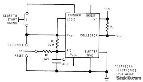
National LM122 timer is connected with manual controls for start, reset, and intermediate termination of 1-h timing cycle started byclosing S1. Once timing starts, S1 has no further effect. Moving S2 up ends cycle prematurely with appropriate change in output state. Moving S2 down resets timing capacitor to 0 V without changing output; releasing S2 starts new timing cycle.-C. Nelson, Versatile Timer Operates from Microseconds to Houm, National Semiconductor, Santa Clara, CA, 1973, AN-97, p 9. (View)
View full Circuit Diagram | Comments | Reading(1075)
PROPERTT_ALARM_CIRCUIT
Published:2009/7/12 22:43:00 Author:May
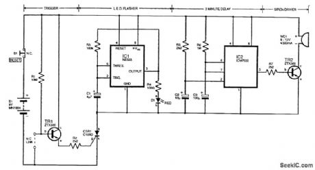
The circuit is designed to protect by means of a wire loop or mercury switch. TR1 and associated components form a switch that is biased off by the normally closed (N.C.) link. When the link is broken, TR1 conducts and triggers the thyristor (CSR1) into conduction. Consequently, the LED flasher centered around the 555 astable of IC1 causes D1 to blink. Additionally, IC2 is a monostable timer that triggers through R5/C2 and drives an audible warning device via TR2 for a period of approximately 2 min before resetting. When the audio alarm has timed out, the LED will continue to flash, and this can be cancelled by opening S1, which resets the thyristor. The quiescent current of the circuit is very low because of the high value of resistor R1. A mercury switch can be used in place of the wire link to act as an antitamper alarm, in which case care must be taken to avoid accidental contact with the mercury bead itself because it is highly toxic.
(View)
View full Circuit Diagram | Comments | Reading(1110)
1_YEAR_TIMER
Published:2009/7/12 22:41:00 Author:May
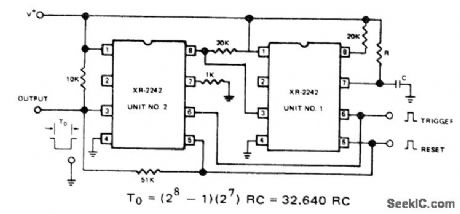
Cascaded operation of Exar XR-2242 long-range timers provides ultralong time delays, up to 1 year, Cascading of counter sections provides 32,640 clock cycles before output pin 3 of unit 2 changes state. Common pull-up resistor makes counter section of unit 2 trigger each time output of unit 1 makes positive-going transition. Cascading additional timer with unit 2 extends time delay to 1.065 x 10⁹RC. With RC values giving 0.1 s, time delay becomes 3.4 years.- Timer Data Book, Exar Integrated Systems, Sunnyvale, CA, 1978, p 19-22. (View)
View full Circuit Diagram | Comments | Reading(1030)
INTERFACE_FOR_AC_LOAD_CONTROL
Published:2009/7/12 22:39:00 Author:May
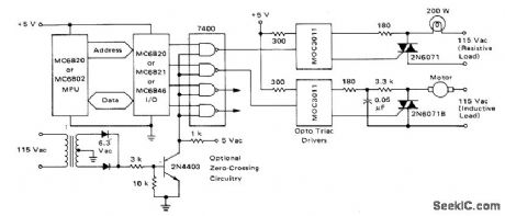
Standard 7400 series gates provide input to Motorola MOC3011 optoisolators for control of triac handling resistive or inductive AC load. Gates are driven by MC6800-type peripheral interface adapters. If second input of two-input gate is tied to simple transistor timing circuit as shown, triac is energized only at zero crossings of AC line voltage. This extends life of incandescent lamps, reduces surge-current effect on triac, and reduces EMI generated by load switching.-P. O'Neil, Applications of the MOC3011 Triac Driver, Motorola, Phoenix, AZ, 1978, AN-780 p 6. (View)
View full Circuit Diagram | Comments | Reading(665)
ANALOG_ELECTRONIC_LOCK
Published:2009/7/12 22:38:00 Author:May
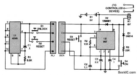
The system is formed of two separate circuits-a key and a keyhole. The key engages the keyhole by means of a mating pair of connectors. The key is a tone-generator circuit consisting of a 4049 hex inverter CMOS IC (U1), switches (S1 and S2), a resistor (R1), and a capacitor (C1). The value of the tone generated by that circuit, in hertz, is determined by 1/(1.4XR1C1) The keyhole is a 567 tone-decoder circuit that can be configured to detect any frequency from 0.01 Hz to 500 kHz. The frequency it detects (fo)is set by resistor R2 and capacitor CZ, according to fo=1.1/(R2C2). When the key is inserted into the lock and switch S1 is pressed, a tone is supplied to the input of the keyhole circuit. If the tone frequency is close enough to fo, the 567IC turns on the relay (K1), which should be connected to the electronic locking device. Components R3 and D1 are used to latch the circuit, so that the output stays on even after the input tone is removed. When S2 is pressed, the system is reset. Switch S3 resets the circuit from inside. Note: The accuracy with which the keyhole circuit detects fo can be set by changing the values of three components. First, R2 should be between 2000 and 20,000 Ω . Second, the value in microfarads of capacitor C4 should be n/fo, where n is a value between 1300 and 0000 (which gives a detection accuracy of up to 14 percent of fo). Finally, capacitor C3 should have about twice the capacitance of capacitor C4. Battery B1 supplies both circuits.
(View)
View full Circuit Diagram | Comments | Reading(1387)
SCR_LAMP_BRIGHTNESS_CONTROL
Published:2009/7/12 22:37:00 Author:May
Will control up to 1.6 amp rms while operating directly from power line, yet is sufficiently compact to fit into base of common household lamp socket.-Low-Cost, Low-Power SCR's to invade Commercial Market, EEE, 13:8, p21-22. (View)
View full Circuit Diagram | Comments | Reading(758)
DIGITAL_LOCK_CIRCUIT
Published:2009/7/12 22:33:00 Author:May
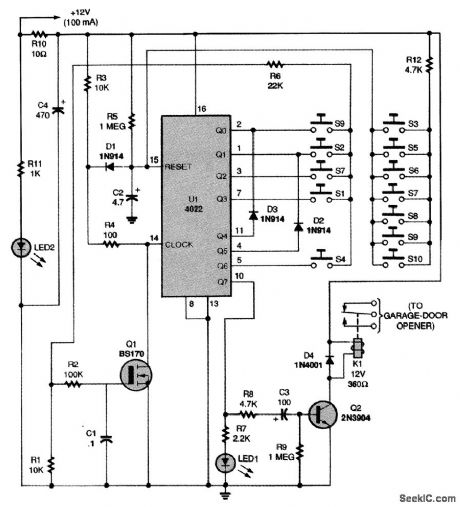
This circuit depends on the entry of a correct sequence code. An incorrect number that is not part of the code causes the circuit to reset. When the correct code is entered, Q2 operates relay K1 for a short time, depending on C3. (View)
View full Circuit Diagram | Comments | Reading(2012)
4_h_SEQUENTIAL_TIMER
Published:2009/7/12 22:32:00 Author:May
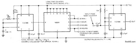
Use of N8281 divider network between sections of 556 dual time gives extremely long timedelays without costly large low-leakage capacitors. First section operates as oscillator having period of 1/f. Oscillator output is applied to divide-by-/N network to give output with period of N/f for triggering second half of timer. Connection of divider to second section determines amount of delay introduced by divider. Cascading of additional dividers increases maximum delay to days or even weeks.- Signetits Analog Data Manual, Signetics, Sunnyvale, CA, 1977, p 724. (View)
View full Circuit Diagram | Comments | Reading(1126)
CHARACTER_GENERATOR_DEFLECTION_SWITCH
Published:2009/7/16 21:50:00 Author:Jessie
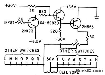
Coarse deflection system uses 32 identical power transistor circuits in switching configuration to drive low-inductance main deflection yoke. Half of these control X deflection to give 16 discrete positions, and the remainder serve for Y deflection.-K. E. Perry and E. J. Aho, Radar-Computer Display Traces Alphanumeric Characters,Electronics, 34:26, p 75-79. (View)
View full Circuit Diagram | Comments | Reading(804)
Overcurrent protection circuit diagram
Published:2011/7/20 5:06:00 Author:nelly | Keyword: Overcurrent, protection
View full Circuit Diagram | Comments | Reading(680)
CUT_PHONE_LINE_ALARM_1
Published:2009/7/12 22:31:00 Author:May
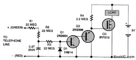
Detecting a cut phone line can be an important function of an electronic security system. UnforLunately, detecting a cut phone line isn't easy because the voltages on a normal phone line vary so rnuch. The voltage is typically 48 Vdc when the telephone is on the hook, 2 to 15 Vdc during a conversation, 90 Vac during ringing, and 200 Vdc when the telephone company is testing the line. Brief moments of 0 V are common; what you really want to detect is a voltage that goes to zero and stays there. A second restriction is that the cut phone line detector cannot draw any appreciable current. Its impedance has to be higher than 50 MΩ or the telephone company will think it's a leaky cable, Components R1, R2, R3, and C1 smooth out momentary variations in voltage so that the alarm doesn't trigger every time the telephone rings. If the voltage stays at zero for 30 s or more, the alarm should trigger. The load can be a piezo buzzer, an optocoupler, or a small relay.Because of the tiny currents it rnust detect, this circuit should be powered by its own 9-V battery, with no direct connection to the rest of the burglar alarm. Otherwise, a slight difference in ground potentials might cause the circuit to perform somewhat erratically. (View)
View full Circuit Diagram | Comments | Reading(1122)
SPARK_MACHINING_CONTROL
Published:2009/7/12 22:31:00 Author:May
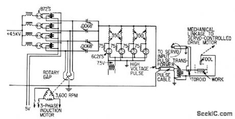
Servo-controlled high-power electric spark machine produces repeated discharges between tool electrode and workpiece to cause erosion of metal to desired shape. Power source is 4.5-KV three-phase rectifer providing peak discharge current of 4,500 amp at pulse repetition rate of 2,880 pps. Rotary gap is used for pulse switching.-E. M. Williams and C. P. Porterfield, Spark Machine Tool has Servo Control, Electronics, 31:43, p90-92. (View)
View full Circuit Diagram | Comments | Reading(1359)
PROSTHETIC_HAND_CONTROL_CIRCUIT
Published:2009/7/16 21:28:00 Author:Jessie
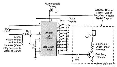
A proposed circuit for the control of an electromechanical prosthetic hand would derive electrical control signals from shoulder movements. The harness would contain a linear potentiometer (R1 in the figure), the resistance of which would be varied by shrugging the shoulder, as in the older mechanical system. The variable output voltage of the potentiometer would be fed to art attenuating potentiometer (R2), which would be set to scale the voltage to the range of shoulder movement. The scaled voltage would be fed to an analog-to-digital converter of the type used to control a bar-graph display. Either a linear or a logarithmic converter could be used, depending on the requirements of the user. Each digital output, in continuous or single-pulse mode, would be fed to a transistor switch, which would supply current to a solenoid or motor to actuate one of the prosthetic fingers. With no shrug, the prosthetic thumb and all of the prosthetic fingers would be extended. As the shrug is increased, the digital outputs would turn on in sequence, thereby causing the thumb and fingers to move sequentially to the closed position. (View)
View full Circuit Diagram | Comments | Reading(1395)
TRIAC_ac_VOLTAGE_CONTROL
Published:2009/7/16 21:27:00 Author:Jessie
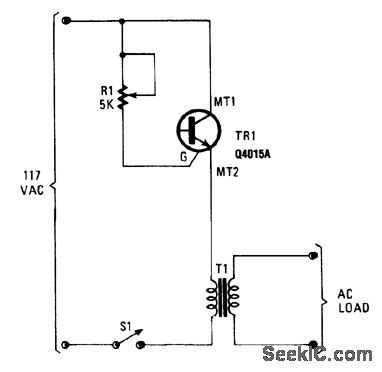
By using a variable resistor in the gate of TR1, variable conduction angles can be achieved via R1. (View)
View full Circuit Diagram | Comments | Reading(837)
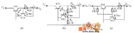
GUARD_DRIVE
Published:2009/7/16 23:30:00 Author:Jessie
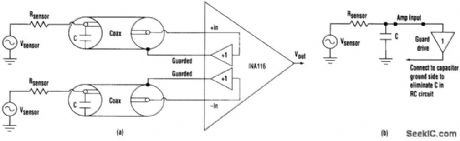
A guard drive can improve common-mode rejection and ac gain when an IA includes an RC circuit made up of the sensor source resistance and the capacitance associated with a coax cable (a). The guard drive prevents a voltage from developing across the capacitance, thus eliminating it from the RC filter's equivalent circuit (b). (View)
View full Circuit Diagram | Comments | Reading(769)
BURGLAR_ALARM
Published:2009/7/12 22:28:00 Author:May
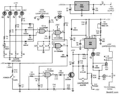
This burglar alarm uses either normally closed (S5 to S8) or normally open (S9 to S11) switches or a combination thereof. Activation sets latches IC1-b and IC1-c. S1 is used to disarm the circuit. IC1-d and related components drive switch Q1, which triggers timer IC2. IC2 generates a pulse, determined by R3 and C5, that energizes alarm relay RY1. S2 allows for a continuous alarm and S12 is a panic switch to sound the alarm immediately. Either a built-in buzzer (BZ1) or an external siren can be used as an annunciator. (View)
View full Circuit Diagram | Comments | Reading(0)
LOW_VOLTAGE_POWER_CONTROLLER
Published:2009/7/12 22:27:00 Author:May
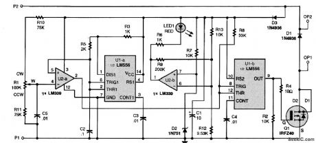
The circuit has a duty-cycle generator that produces an output varying from fully off to fully on and pulses of any duty cycle in between the two extremes. The circuit can be fed from any dc supply source of between 10 and 15 V. U1-a and U2-a combine to form a voltage-to-pulse-width converter. The first half of the dual oscillator/timer is configured as an astable oscillator, generating a continuously oscillating ramp voltage, Op amp U2-a compares the voltage at its noninverting input to the voltage at its inverting input. The op amp will give a low output if R1's wiper voltage is higher than the instantaneous voltage present at pins 2 and 6 of U1-a. The output of U2-a at pin 2 will have an on/off ratio that is proportional to the voltage at RI's wiper. Because the output of U2-a does not have enough power-handling capacity to drive the MOSFET its output is fed to U1-b, which is used to bufferthe signal. The low-impedance, pulsed output of U1-b at pin 9 is fed to the gate of MOSFET Q1, driving it hard on or off. Diode D1 is used to suppress the reverse-voltage spikes generated by inductive loads during turn-off. If the circuit will not be used to drive inductive loads (motors), D1 can be eliminated. Note: This controller can be used only with incandescent lamps and permanent-magnet dc motors. (View)
View full Circuit Diagram | Comments | Reading(0)
LINEAR_PULSE_WIDTH_CONTROL
Published:2009/7/16 23:28:00 Author:Jessie
Blanking pulse generator provides blanking signal starting with input pulse and remaining on for some nominal portion of pulse, regardless of dropouts due to noise in triggering pulse.-blanking Pulse Generator with Linear Pulse Width Control, Electronic Circuit Design Handbook, Mactier Pub. Corp., N.Y., 1965, p 78. (View)
View full Circuit Diagram | Comments | Reading(676)
BISTABLE_INDICATOR_LAMP_DRIVER
Published:2009/7/16 23:18:00 Author:Jessie
Permits controlling lamp with short trigger pulses, for control panel of computer. Negative 2-V trigger at A turns on lamp, which then remains on due to regenerative feedback in circuit. Positive pulse at A turns out lamp. Use of complementary-type transistors minimizes standby power when lamp is out.- Transistor Manual, Seventh Edition, General Electric Co., 1964, p 202. (View)
View full Circuit Diagram | Comments | Reading(890)
| Pages:108/312 At 20101102103104105106107108109110111112113114115116117118119120Under 20 |
Circuit Categories
power supply circuit
Amplifier Circuit
Basic Circuit
LED and Light Circuit
Sensor Circuit
Signal Processing
Electrical Equipment Circuit
Control Circuit
Remote Control Circuit
A/D-D/A Converter Circuit
Audio Circuit
Measuring and Test Circuit
Communication Circuit
Computer-Related Circuit
555 Circuit
Automotive Circuit
Repairing Circuit