
Control Circuit
Index 112
FAN_SPEED_CONTROL
Published:2009/7/17 4:14:00 Author:Jessie
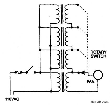
Several 24-V 1.5-A transformers can be used as a speed control, where a triac would be usable,such as on an induction motor. Connect the primaries in parallel and shown. (View)
View full Circuit Diagram | Comments | Reading(725)
BLOOD_FLOW_CONTROL
Published:2009/7/17 4:40:00 Author:Jessie
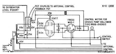
Used to correct long-term differences in flow rates of venous one arterial pumps. Venous control portion of heart-lung amplifier has two inputs, a signal derived from oxygenator level error and an input from potentiometer connected to arterial transmission control lever.-R. Roberts und J. Loeffler, Automatically Controlled Heart-Lung Machine, Electronics, 33:31, p 91-93. (View)
View full Circuit Diagram | Comments | Reading(718)
Heart_rate_monitor
Published:2009/7/17 4:34:00 Author:Jessie
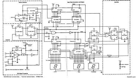
Heart rate monitor (courtesy Motorola Semiconductor Products Inc.). (View)
View full Circuit Diagram | Comments | Reading(4272)
TELEPHONE_OPERATED_ac_POWER_SWITCH
Published:2009/7/10 21:35:00 Author:May
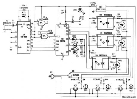
Tones (from the DTMF) on the telephone line are detected by U1. When a valid tone is received, pin 14 (D/V) of U1 produces a positive pulse that is used to drive NAND gates U2A and U2B and then to latch binary data from U1 into Quad-D flip-flop U3 (U1 could be decoded into 16 bits, if required). The Q outputs of U3 drive optoisolators that control triacs TR1, TR2, and TR3. PS1 is a 6-V 150-mA dc adapter that operates from 120 Vac. (View)
View full Circuit Diagram | Comments | Reading(1440)
YOKE_DRIVER
Published:2009/7/17 4:23:00 Author:Jessie
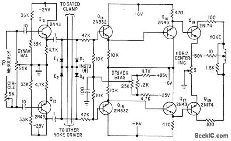
Used to damp sweep signal voltage to reference voltage during clamping time at end of sweep, while removing clamp during sweep. Diodes D1-D2 and D3-D4, con netted in opposite polarity to each signal line, serve as clamp circuit.-C. E. Veazie, Transistorized Radar Sweep Circuits Using Low Power, Electronics, 32:26, p 46-47. (View)
View full Circuit Diagram | Comments | Reading(755)
INCUBATOR_MOTOR_CONTROLLER
Published:2009/7/17 4:17:00 Author:Jessie
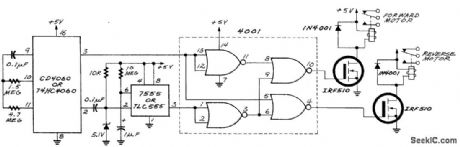
The circuit has a 4060 CMOS long-period timer, which consists of an oscillator plus a series of binary counters that divide the frequency by 2, 4, 8, etc. up to 16,384. The oscillator runs at a comfortable 2 Hz (2 cycles per second), controlled by a capacitor and two resistors, and the binary counter divides this to produce a square wave that has only one cycle every 2 hours, as well as another one that oscillates twice as fast. The faster of the two square waves determines when the motor runs, and the slower one determines its direction. Here's how it's done: First, the faster square wave goes through a capacitor, resistor, and diode, which convert it into a narrow negative-going pulse that occurs once per hour. The 555, connected as a monostable, stretches the short pulse so that it is 10 s long (the length of time the motor should run). Logic gates then steer that pulse to one of two relays so that the motor runs either forward or backward, depending on which state the slow square wave is in at the time. Because the forward and reverse pulses are generated by the same 555 circuit, they are the same length-this is important so that the reverse cycle will exactly undo the motion of the forward cycle. (View)
View full Circuit Diagram | Comments | Reading(2047)
BOUNCE_FREE_AUTO_REPEAT_SWITCH
Published:2009/7/10 21:17:00 Author:May
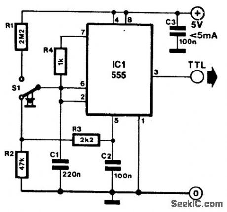
This switch that keeps pulsing as long as it is pressed is often required. The circuit here used the well known Type 555 for this purpose. Its output is a TTL-compatible signal. Pin 5 of the timer has a potential of 67% of the supply voltage, UCC In the quiescent condition (switch not pressed), C1 charges via R2 and R3 to a voltage that is lower than that at pin 5, and thus is also lower than the toggle voltage.When the switch is pressed, C1 is rapidly charged via R1 to the toggle voltage, upon which the timer emits a pulse. At the same time, the capacitor is discharged again via R4. As long as the switch is pressed, the circuit functions as an astable toggle and produces pulses. When it is released, the capacitor cannot charge to the toggle voltage. (View)
View full Circuit Diagram | Comments | Reading(833)
6_DIGIT_VALUES
Published:2009/7/10 21:14:00 Author:May
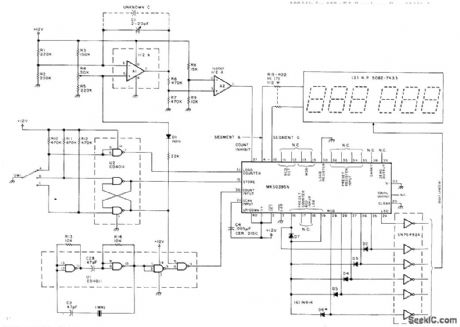
Digital capacitance meter provides display of capacitance values from 1 pF to 999999 pF (1.0μF). Start-measurement switch drains charge from capacitor under measurement and diverts constant-current source to ground. Capacitor begins charging,and counter accumulates 1-μs pulses from crystal clock. When capacitor charge voltage reaches threshold of countinhibit line for counter, contents of counter are displayed as capacitance value. Circuit uses Mostek MK50395N six-decade counter that provides ;-segment output data for display. Position A of SW1 is starting point B stores data in counter display after capacitor measurement, and C initiates measurement. Display includes leading-zero suppression.-J. Garrett,What's Your μF?, 73 Magazine, Dec. 1978, p 234-235. (View)
View full Circuit Diagram | Comments | Reading(3537)
SWITCHING_CIRCUIT
Published:2009/7/10 20:57:00 Author:May

This switching circuit acts like a bank of interlocked mechanical switches; pushing one of the buttons latches its corresponding output and unlatches a previously selected output. A pair of inverters forms a latch for each output.Pressing button B1, for example, applies a positive pulse, via resistor diode D1B, to the input of the first output's, 0UT1, latch. This positive pulse will set OUT1 high. Feedback locks OUT1's pair of converters in this HIGH state. Meanwhile, the pulse will also pass through diode D1A to the differentiator that is formed by C and R2. The differentiator will shorten the pulse.The shortened pulse goes to all the latches and resets all of them, except the latch that sees the longer setting pulse. Obviously, if you press more than one button at once, more than one output will latch at once. (View)
View full Circuit Diagram | Comments | Reading(1267)
ON_OFF_SWITCH
Published:2009/7/10 20:54:00 Author:May
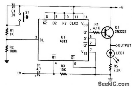
A CD 4013 dual-D flip-flop is used to drive an emitter-follower. This circuit can be used where a simple pushbutton on/off is desired. (View)
View full Circuit Diagram | Comments | Reading(7588)
SATELLITE_TV_AUDIO_SWITCHER
Published:2009/7/10 20:52:00 Author:May
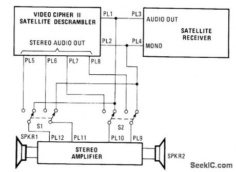
Some channels offer a separate audio mode (SAP) in a second language. It is usually transmitted on 6.8 MHz, which is the frequency used for unscrambled channels. The audio in the scrambled channels is transmitted along with the picture, so when the descrambler descrambles the signal, it also descrambles the audio in stereo. When the channel offers SAP, you'll find it on 6.8 MHz.The switches are a pair of DPDT switches that have the toggle handles tied together. In one position, you hear the audio in stereo and in the other position, you hear the SAP. Just turn down the volume level on the TV and you can connect it to a stereo amplifier and a pair of speakers. (View)
View full Circuit Diagram | Comments | Reading(775)
DIODE_RF_SWITCH
Published:2009/7/10 20:47:00 Author:May
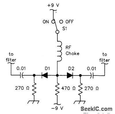
D1 and D2 can be IN914B- or HP2800-senesdiodes(for UHF).The loss is over 60 dB h the OFF state,and less than 3 dB at 3.5 to 30 MHz(using common IN914B diodes). (View)
View full Circuit Diagram | Comments | Reading(870)
PRECISION_NARROW_BAND_TONE_SWITCH
Published:2009/7/10 20:43:00 Author:May
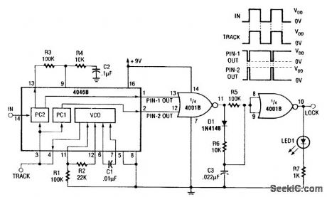
This signal tracker and lock detector combine to make a precision tone switch. Filter R3/R4/C2 determines signal capture and tracking range, as well as settling time.. Max. VCO frequency: R1C1. Min. VCO frequency: (R1+R2)C2Pin 9 voltage affects both. The minimum at pin 9 is 0 V and the maximum at pin 9 is VDD. In the lock detector, the PC (phase comparator) outputs are pulses whose width is proportional to the phase difference between the two PC inputs. At lock up, the two PC outputs are almost mirror images. The output of IC1A remains low and IC1B is high. This lights LED1. If the loop is unlocked, the LED will not light. (View)
View full Circuit Diagram | Comments | Reading(759)
SCR_OVERVOLTAGE_PROTECTOR
Published:2009/7/10 20:37:00 Author:May
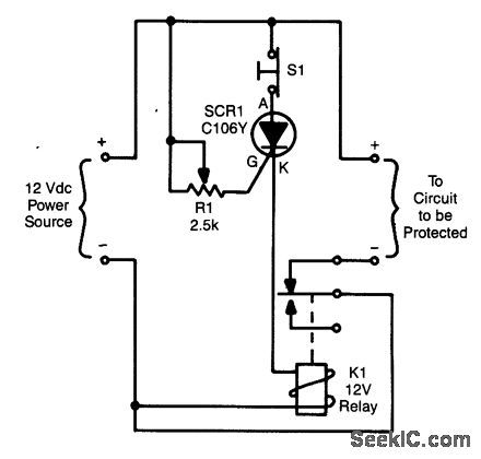
Depending on the setting of R1, when the voltage exceeds a certain amount, SCR1 triggers, which activates K1 and opens the circuit. S1 resets the SCR. (View)
View full Circuit Diagram | Comments | Reading(1017)
BANG_BANG_CONTROLLERS
Published:2009/7/10 20:32:00 Author:May
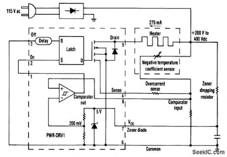
Just one chip, the PWR-DRV1 from Power Integrations, builds a bang-bang controller that switches 275 mA and runs off the rectified 115-Vac mains. An on-chip zener diode powers the chip from high voltage through a dropping resistor. (View)
View full Circuit Diagram | Comments | Reading(779)
BALANCE_AND_LOUDNESS_CONTROL
Published:2009/7/10 6:13:00 Author:May
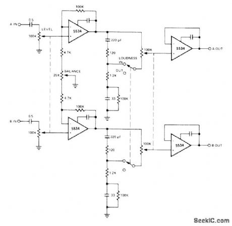
Provides bass boost at low listening levels to compensate for nonlinearity of human hearing sys-tem. Balance control permits equalizing volume from left and right loudspeakers at particular listening location.- Signetics Analog Data Manual, Signetics, Sunnyvale, CA, 1977, p 640. (View)
View full Circuit Diagram | Comments | Reading(1081)
ACTIVE_MIDRANGE_TONE_CONTROL
Published:2009/7/10 6:10:00 Author:May
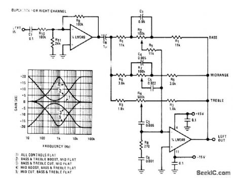
Addition of midrange tone control to active bass and treble control gives greater control flexibility. Center frequency of midrange control is determined by C4 and C5 and is 1 kHz for values shown. C5 should have 5 times value of C4.-“Audio Handbook,” National Semiconductor, Santa Clara, CA, 1977, p 2-40-2-49. (View)
View full Circuit Diagram | Comments | Reading(2195)
PREAMP_WITH_TONE_CONTROLS
Published:2009/7/10 6:08:00 Author:May
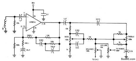
Use of LM381A selected low-noise preamp with passive bass and treble tone controls as phono or tape preamp gives superior noise performance while eliminating need for transistor to off set signal loss in passive controls Circuit provides 20-dB boost and cut at 50 Hz and 10 kHz relative to midband gain, Design equations are given. Use log pots for tone controls. Other stereo channel is identical. Controls are ganged.- Audio Handbook, National Semiconductor, Santa Clara, CA, 1977, p 2-40-2-49. (View)
View full Circuit Diagram | Comments | Reading(2828)
ACTIVE_TONE_CONTROLS
Published:2009/7/10 6:03:00 Author:May
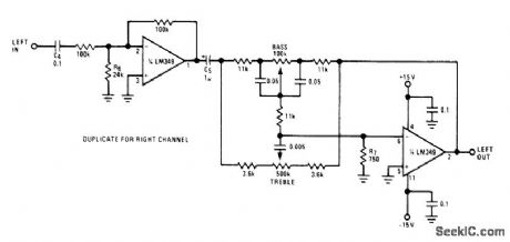
Provides ±20 dB gain with 3-dB corners at 30 and 10,000Hz,Use of LM349 quad opamp means only one IC is needed for both stereo channels, Buffer at input gives high input impedance (100k) for source, Total harmonic distortion is typically 0.05% across audio band Input-to-output gain is at least 5.-“Audio Handbook,” National Semiconductor, Santa Clara, CA, 1977,p 2-40-2-49. (View)
View full Circuit Diagram | Comments | Reading(1127)
Light_operated_6_kV_series_switch_for_high_voltage_crowbar_circuits_or_high_voltage_pulse_forming_networks
Published:2009/7/17 5:17:00 Author:Jessie
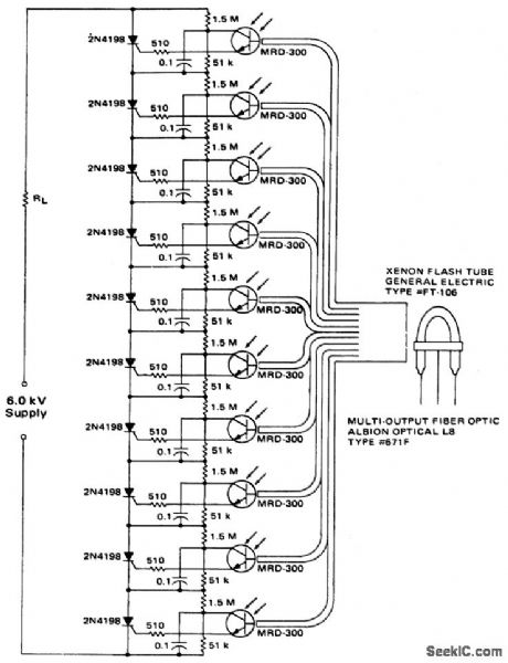
Light-operated 6 kV series switch for high-voltage crowbar circuits or high-voltage pulse-forming networks(courtesy Motorola Semiconductor Products Inc.). (View)
View full Circuit Diagram | Comments | Reading(706)
| Pages:112/312 At 20101102103104105106107108109110111112113114115116117118119120Under 20 |
Circuit Categories
power supply circuit
Amplifier Circuit
Basic Circuit
LED and Light Circuit
Sensor Circuit
Signal Processing
Electrical Equipment Circuit
Control Circuit
Remote Control Circuit
A/D-D/A Converter Circuit
Audio Circuit
Measuring and Test Circuit
Communication Circuit
Computer-Related Circuit
555 Circuit
Automotive Circuit
Repairing Circuit