
Control Circuit
Index 121
High power DC motor over-current protection circuit diagram
Published:2011/8/2 2:56:00 Author:Rebekka | Keyword: High power DC, motor over-current protection
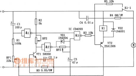
In order to prevent the motor generating high current and make the circuit work inappropriately. the Cl, Rl, RPl and NAND gate form the starting protection time delay circuit. When the motor starts, there is not voltage at Cl. At this time NAND gate 1 outputs low level, NAND gate 3 outputs high level, it makes the VT2 in the off mode, then the relay Kl does not work, andits contact stillkeeps the closed mode. The DC motor gets normal power supply. When the Cl terminal voltage rises gradually to a certain value, the NAND gate 1 is overturned, the output terminal turns to high level, the start protection circuit stops to work. After that the output mode of NAND gate 3 is the current detection circuit control composed of the RP2, R2, VTl and Ro. (View)
View full Circuit Diagram | Comments | Reading(3443)
Temporary power failure protection and death protection circuit diagram
Published:2011/8/2 2:52:00 Author:Rebekka | Keyword: Temporary power failure protection , death protection
Most of the over-current, overvoltage protection of the power supply will stop working after the power failure, the output will be zero, and then it can be manually reset to work again; Or it only has temporary protection that will stop the power output after the failure happened. After the delay time, the power supply will automatically return to work. But in many devices, they require temporary protection and the die protection. For example, it requires the power to allow the load transient ignition and overcurrent. (View)
View full Circuit Diagram | Comments | Reading(774)
ULTRASONIC_PEST_CONTROLLER
Published:2009/7/9 1:10:00 Author:May
This circuit consists of two basic parts: an oscillator tuned to 40 kHz, and a voltage doubler with pulse generator. The pulses are about 10 ms long and occur 2 -3 per s to reduce battery drain and increase the annoyance factor for a cat, dog, hedgehog, etc. The voltage doubling action increases the available output power for any given battery voltage. (View)
View full Circuit Diagram | Comments | Reading(929)
ULTRASONIC-PULSED_PEST_CONTROLLER
Published:2009/7/9 1:07:00 Author:May
IC2 forms a stable oscillator whose frequency and pulse width is determined by the values of R4, R5, R6, and C4. R4 is made adjustable for precise frequency setting. The output of IC2 is pin 3, which is capacitively coupled to the base of Q1. L1 acts as a high-impedance choke to the signal, while allowing the collector of Q1 to be dc-biased. Q1 amplifies the positive pulses from IC2 and step drives the series resonant combination of L2 and TD1. Resistor R10 serves to broaden the response of this resonant circuit. L2 and the inherent capacity of the transducer, TD1, forms a resonant circuit at around 23 kHz. It is usually found that most rodents are bothered when the signal is pulsed with the off exceeding the on time. This timing is accomplished via timer IC1 and timer inverter Q2. IC1 is free running and its periods are determined by R1, R2, and C2 to be approximately two seconds off and two seconds on. The periods are inverted via Q2 and used to gate pin 4 of IC2, the frequency oscillator, tuming it on for two seconds and off for three seconds. The power supply is a conventional voltage doubler with a zener regulator for the oscillator voltages. (View)
View full Circuit Diagram | Comments | Reading(1092)
Machine tool magnetic chuck undercurrent protection circuit diagram
Published:2011/8/2 2:43:00 Author:Rebekka | Keyword: Machine tool magnetic chuck , undercurrent protection
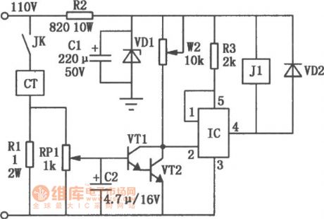
The signal from the sampling circuit is amplified by voltage, whichmakes the collector potential of VTl, VT2 close to 0V, the ② pin of IC's is at the low potential , ④ pin is turned on, relay J1 gets the power. The dynamic co-contact is closed, so that the machine starts to work. When the magnetic chuck current is less than 90% of rated current (this value is adjustable), IC's ④ pin is stopped. J1 is off, the machine feed-through circuit is off at the same time. The feed-though system stops working, thus avoids the accident. This circuit IC uses TWH8751 type, VTl uses 9013-type, VT2 uses 3DGl2 type, VDl uses 24V, 1W. VD2 uses lN4148 type, relay J1 uses JTX-24 type. (View)
View full Circuit Diagram | Comments | Reading(1851)
SOLID_STATE_RELAY
Published:2009/7/9 0:49:00 Author:May
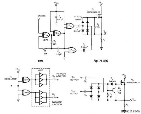
A power MOSFET and a quad exclusive-OR oscillator makes an effective solid-state relay. Figure 75-S(a)'s capacitively isolated drive circuit provides gate drive to turn on the n-channel device. This con-sists of a gated oscillator (IC1A and IC1B running at 500 kHz, set by R1, R2, and C1).The diode bridge (D1 through D4) rectifies the charge transferred through C2 and C3. When you dis-able the oscillator, R3 discharges the stored gate charge, thereby turning off the MOSFET. R3 needs to allow fast turn-off times without loading the gate's enhancement voltage. A value of 10-k0 is sufficient to produce a turn-off time of 800 ;ts with an 18-mΩ SMP60N06-18 MOSFET. The measured turn-on time is 150 μs.You can reduce the turn-off time to 100 pts by using a pnp transistor as a diode-steering emitter-fol-lower in the MOSFET gate circuit (Fig. 75-5(b)). Adding a hex buffer to Fig. 75-5A's circuit increases the drive capability of the complementary outputs (Fig. 75-5(c)). (View)
View full Circuit Diagram | Comments | Reading(3139)
DELAY_OFF_RELAY_CIRCUIT
Published:2009/7/9 0:45:00 Author:May

When voltage is applied to the capacitor, it charges. While it's charging, the relay remains latched. When the charging current falls below the level needed to hold the relay down, the relay unlatches. The higher the value of the capacitor, the longer the relay will remain latched. (View)
View full Circuit Diagram | Comments | Reading(1117)
LOW_CONSUMPTION_MONOSTABLE_RELAY
Published:2009/7/9 0:44:00 Author:May
A monostable relay has two states: operative when a large enough current flows through its coil and quiescent when no current flows. A relay contact that assumes a certain position after the supply voltage has been switched on is required in many applications. Of course, many relays operate in that manner.However, most of these relays require an energizing current of 50 mA or more and that normally pre-cludes a battery supply. The circuit presented here, which uses a bistable relay, can solve that problem.The contact of a bistable relay normally remains in the position it is in after the supply is switched off. This circuit, however, makes the bistable relay behave like a monostable type, at a modest current.When the supply voltage is switched on, C1 charges via D1 and the relay coil. The current then flow-ing through the coil causes the relay contact to assume one of two positions. The forward drop across D1 ensures that the base of T1 (in this condition) is more positive than its emitter so that T1, and thus T2, is switched off.When the supply voltage is switched off, the emitter of T1 is connected to the positive terminal of C1, while the base is connected to the negative terminal of the capacitor via R1 and the relay coil. This results in T1, and thus T2, switching on so that C1 discharges via T4 and the relay. The current flows through the relay coil, then ftows in an opposite direction and this causes the contact to change oven The bistable relay thus behaves exactly as a monostable with the advantage, however, that the opera-tional current is determined by R1, which amounts to only 130 μA. To ensure reliable operation, the rating of the relay coil should be 65 to 75% of the supply voltage. In the prototype, a 9-V relay was used with a battery supply voltage of 12 V. (View)
View full Circuit Diagram | Comments | Reading(1963)
BIDIRECTIONAL_SWITCH
Published:2009/7/9 0:42:00 Author:May
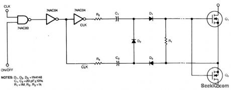
Using voltage doublers, this simple switch circuit uses a clock signal and a control signal to switch MOSFETs. (View)
View full Circuit Diagram | Comments | Reading(904)
SONAR_TRANSDUCER_SWITCH
Published:2009/7/9 0:42:00 Author:May
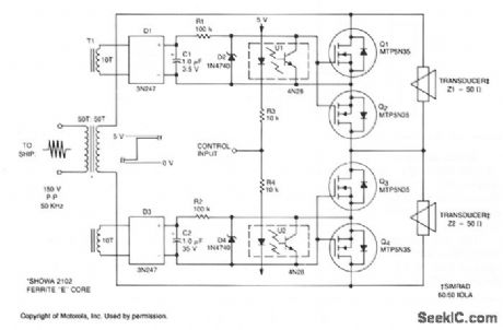
This submersible sonar positioning apparatus generally consists of dual-opposed ultrasonic transducers, alternately excited, with return signals processed and displayed for observation and measurement. Typical transmitter frequencies range from 50 to 200 kHz and pulse widths can be varied from 0.3 to 5 ms, depending on depth and resolution requirements.The input to the transducer/switch is transformer T1 which provides isolation and impedance matching. The turn ratio of the secondary windings depends on the peak-to-peak amplitude of the transmitter output into the specified load. The transmitted pulse that appears on the secondary winding charges capacitors C1 and C2 through bridge rectifiers D1 and D3. Zener diodes D2 and D4 limit the TMOS gate bias to 12 V; R1 and R2 limit the discharge current from C1 and C2.The square-wave control input is applied to opto-isolators U1 and U2 through resistors R3 and R4. If the control input is O V, U1 is activated; when it changes to + 5 V, U2 is activated. When U1 is activated, it saturates and reduces the gate bias to zero, turning Q1 and Q2 off. Q3 and Q4 remain on, effectively shunting transducer 22. When U2 is activated, it saturates and reduces the bias to zero, turning Q3 and Q4 off. Q1 and Q2 remain on, effectively shunting transducer Z1. (View)
View full Circuit Diagram | Comments | Reading(2681)
LATCHING_ac_SOLID_STATE_RELAY
Published:2009/7/9 0:41:00 Author:May
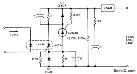
Latching is obtained by storing the gate trigger energy from the preceding half cycle in the capacitors. Power must be interrupted for more than one full cycle of the line to ensure turn-off. Resistor R and capacitor C are chosen to minimize dissipation, while assuring triggering of the respective SCRs for each cycle. A pulse of current, over 10 ms duration into the H11C4 IRED, ensures triggering the latching relay into conduction. (View)
View full Circuit Diagram | Comments | Reading(1447)
LAMP_DRIVE
Published:2009/7/20 20:55:00 Author:Jessie
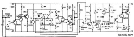
Count-rate meter of radiation-detecting tumor stunner provides input signal for d-c amplifier. Controls R1 and R2in difference amplifier provides zero suppression and R3 provides scale expansion. Circuit drives lamp that exposes film in step with scanning motion of probe.-E. Gordy and G. Sieber, Sensitive Amplifier Helps Lo-Gale Tumors, Electronics, 34:1, p 123-124. (View)
View full Circuit Diagram | Comments | Reading(759)
STEP_SERVO_CONTROL
Published:2009/7/21 1:16:00 Author:Jessie
Variable UJT oscillator generates train of pulses under control of digital input logic levels, at 1000 pulses per second for logic 1 or 4400 pulses per second for logic 0, with smooth transitions between rates when logic changes, for driving stepping servomotor. Q1 and Q2 are constant-current sources. JFET Q3 acts as voltage-controlled variable resistor in parallel with R10, controlling pulse rate of UJT oscillator Q4.-C.R.Forbes.Step-Servo Motor Slew Generator. EEE Magazine.Oct.1970,p76-77. (View)
View full Circuit Diagram | Comments | Reading(822)
TWO_PHASE_SERVO_DRIVE
Published:2009/7/21 1:17:00 Author:Jessie
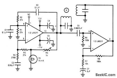
Both sections of National LM377 power amplifier are connected to provide up to 3 W per phase for driving small 60-Hz two-phase servomotor. Power is sufficient for phonograph turntable drive. Lamp is used in simple amplitude stabilization loop. Motor windings are 8 ohms, tuned to 60 Hz with shunt capacitors.- Audio Handbook, National Semiconductor, Santa Clara, CA, 1977, p 4-8-4-20. (View)
View full Circuit Diagram | Comments | Reading(873)
OVERLOAD_PROTECTION
Published:2009/7/8 23:15:00 Author:May
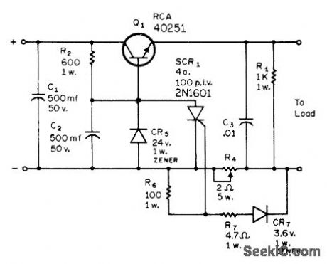
When critical current is exceeded, SCR1 condtlcts and reduces base-ground voltage of Q1 cutting it off. Load current then drops to very low value, and Q1 is protected. Operation is restored by turning off current supply to power transformer after clearing short-circuit condition.-R. Phelps, Jr., Protective Circuits for Transistor Power Supplies, CQ March 1973, p 44-48 and 92. (View)
View full Circuit Diagram | Comments | Reading(0)
Three-phase motor phase failure protection circuit diagram
Published:2011/8/2 2:23:00 Author:Rebekka | Keyword: Three-phase motor, phase failure protection
The circuit is composed of general purpose integrated operational amplifiers. The circuit is shown as above. It can be used in a variety of three-phase motor phase protections. IC uses a typical general-purpose integrated operational amplifiers, such as 5G24, BG305, FC4, F006, XFC77 or other foreign products μA741 etc. The relay J can use DC l2V operating voltage, the DC resistance is 200Ω DC relay. (View)
View full Circuit Diagram | Comments | Reading(3905)
Pulse_position_modulator_using_an_ECG955M_timer
Published:2009/7/21 2:43:00 Author:Jessie
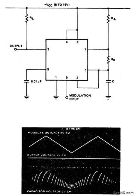
Pulse position modulator using an ECG955M timer/oscillator chip. The timer is connected as an astable multivibrator. With a modulating signal applied to pin 5 the pulse positon will vary with the modulating signal (courtesy GTE Sylvania Incorporated). (View)
View full Circuit Diagram | Comments | Reading(724)
Automatic reset over-voltage protection circuit diagram
Published:2011/8/3 2:40:00 Author:Rebekka | Keyword: Automatic reset, Over-voltage protection
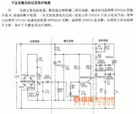
The circuit includes 3 circuit parts:power supply, trigger start and control. The power supply switch of the load R1 is controlled by bidirectional thyristor ZN6346. When the AC voltage is over high, the A point voltage of steady flow component 1N5314 will rise and the unidirectional thyristor will be conducted and the transistor will be closed. The main bidirectional thyristor will be closed at the same time, the load will be protected from damaging. (View)
View full Circuit Diagram | Comments | Reading(1279)
Storehouse temperature measurement alarm circuit diagram
Published:2011/8/3 2:41:00 Author:Rebekka | Keyword: Storehouse temperature measurement alarm
View full Circuit Diagram | Comments | Reading(666)
Inexpensive_high_performance_gain_control_circuit
Published:2009/7/21 2:56:00 Author:Jessie
Inexpensive high-performance gain control circuit (courtesy Analog Devices, Inc.). (View)
View full Circuit Diagram | Comments | Reading(631)
| Pages:121/312 At 20121122123124125126127128129130131132133134135136137138139140Under 20 |
Circuit Categories
power supply circuit
Amplifier Circuit
Basic Circuit
LED and Light Circuit
Sensor Circuit
Signal Processing
Electrical Equipment Circuit
Control Circuit
Remote Control Circuit
A/D-D/A Converter Circuit
Audio Circuit
Measuring and Test Circuit
Communication Circuit
Computer-Related Circuit
555 Circuit
Automotive Circuit
Repairing Circuit