
Control Circuit
Index 127
SUPPLY_OVERLOAD_AND_REVERSE_POLARITY_PROTECTION
Published:2009/7/21 10:03:00 Author:Jessie
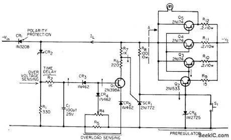
Uses signal from Q1 to trigger SCR1, which turns off series-pass transistor when overload reaches 15 amp. Will also provide limiting of output voltage at 25 V, input overvoltage protection at 32 V, and input reverse-polarity protection by CRL. -J. J. Rado, Versatile SCR Protection for Power Supplies, EEE, 13:8, p 56-62. (View)
View full Circuit Diagram | Comments | Reading(1213)
ADJUSTABLE_SCHMITT_TRIGGER
Published:2009/7/21 9:21:00 Author:Jessie
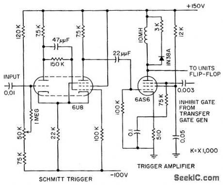
Accepts either sine waves or pulses. Adjustable input level control allows trigger to occur on any desired portion of input waveform. Amplifier stage drives flip-flop of units decade counter directly.-R. W. Wolfe, Decode Decimal Counter Speeds Printed Readout, Electronics, 31;3, p 88-90. (View)
View full Circuit Diagram | Comments | Reading(1040)
TOUCH_SWITCH
Published:2009/7/7 5:38:00 Author:May
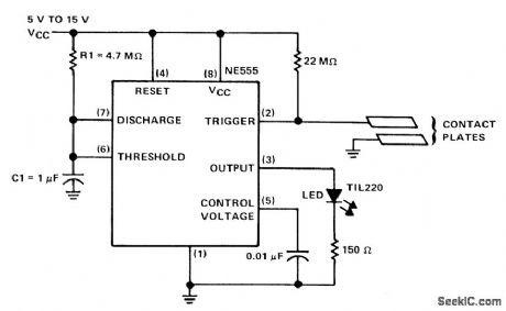
The circuit is basically a NE555 monostable, the only major difference being its method of triggering. The trigger input is biased to a high value by the 22 M ohm resistor. When the contact plates are touched, the skin resistance of the operator will lower the overall impedance from pin 2 to ground. This action will reduce the voltage at the trigger input to below the 1/3 VCC trigger threshold and the timer will start. The output pulse width will be T = 1.1 R1C1, in this circuit about 5 seconds. A relay connected from pin 3 to ground instead of the LED and resistor could be used to perform a switching function. (View)
View full Circuit Diagram | Comments | Reading(0)
TOUCH_ON_OFF_SWITCH
Published:2009/7/7 5:36:00 Author:May
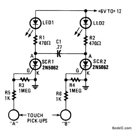
If a Touch On/Off Switch is desired, this circuit fills the bill. Two sensitive gate SCRs are interconnected, so that when one of the devices is turned on, the other (if on) is forced off. That toggling effect gives an on/off circuit condition for each of the LEDs in the SCR-anode circuits. To turn LED1 on and LED2 off, simply touch the A terminal, and to turn LED1 off and LED2 on, the B pick-up must be touched. It is possible to simultaneously touch both terminals, causing both SCRs to turn on together. To reset the circuit to the normal one-on/one-off condition, momentarily interrupt the circuit's dc power source. Additional circuitry can be connected to the anode circuit of either or both SCRs to be controlled by the on/off function of the touch switch. (View)
View full Circuit Diagram | Comments | Reading(1769)
PASSIVE_TONE_CONTROL_CIRCUIT
Published:2009/7/7 5:35:00 Author:May
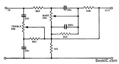
A simple circuit using two potentiometers and easily available standard value components provides tone control. The impedance level is suitable for low-level transistor or op amp circuitry. (View)
View full Circuit Diagram | Comments | Reading(2078)
MIKE_PREAMP_WITH_TONE_CONTROL
Published:2009/7/7 5:33:00 Author:May
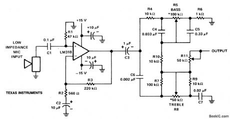
The LM318 op amp is operated as a standard noninverting amplifier. Resistor R1 (47 k ohm) provides an input path to ground for the bias current of the non-inverting input. The combination of R2 (560 ohm) and C2 (10 μF) provides a frequency roll-off below 30 Hz. At 30 Hz and above the gain is relatively flat at about 50 dB, set by the ratio R3/R2. R3 (200 k ohm) furnishes negative feedback from the output to the inverting input of the op amp. C3 (1.0 μF electrolytic) ac couples the preamp to the tone control section. The top half of the tone control section is the bass control. The bottom half controls the treble frequency response. These tone controls (R5 and R8) require audio taper (logarithmic) potentiometers. The 50 k ohm potentiometer on the output can be used to set the output or gain of the preamp. (View)
View full Circuit Diagram | Comments | Reading(2815)
MODEL_RAILROAD_SWITCHING_
Published:2009/7/7 5:05:00 Author:May
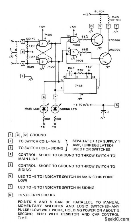
Control circuitis used to drive solenoid-operated track Switches oftγpical HO train layout Inputcan be ρair of comρlementary TTL signals from 8008 orother computer or can be from manual switch s1. 74121 mono MVBR controls time that witch is energized in given direction. Outputcult transistors are rated at 20 W,enough for driving solenoids taking 1 A at 12 V Use protective diodes across coils of solenoids,-H,De Monstoy,Model Railroad Switch Control Circuit,BYTE,Oct .1975,p 87. (View)
View full Circuit Diagram | Comments | Reading(964)
LOGIC_SIGNALS_CONTROL_TDM
Published:2009/7/7 5:03:00 Author:May
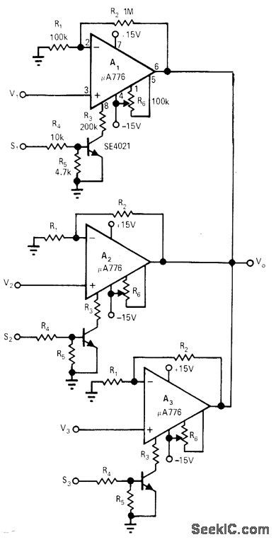
se of μA776 opamps eliminates need for FET switches in time-division multiplexing and signal conditioning. Multiplex inputs S1-S2-S3 can be driven directly by TTL or DTL devices. Each amplifier is controlled by either supplying or denying its 70-μA master-bias input, thus turning it on or off. All stages have identical component values.-M. K. Vander Kooi, Multiplexing Without FETs, EDN/EEE Magazine, Aug. 1, 1971,p47. (View)
View full Circuit Diagram | Comments | Reading(722)
Solid_state_time_delay
Published:2009/7/22 3:48:00 Author:Jessie
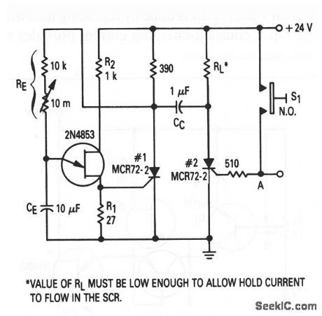
This circuit shows the basic UJT building block (Fig. 9-1), which is used to provide a time-delay function. The circuit is similar to that of Fig. 9-13, except that the mechanical relay is replaced by an SCR (which generally reduces circuit cost). When S1 is pushed, or when a positive-going pulse is applied at point A, SCR#2 turns on and SCR#1 is turned off by CC. With SCR#1 off, the supply voltage is applied to RE, and the circuit begins to time. After a period (determined by the setting of RE), the UJT fires and turns SCR#1 on and SCR#2 off. With the values shown, time delay can be varied from about 1 s to over 2 min. (View)
View full Circuit Diagram | Comments | Reading(1092)
_TONE_CONTROL
Published:2009/7/7 5:03:00 Author:May


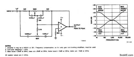
Tone control of audio systems involves altering the flat response ul order to attain more low frequenctes or more high ones,ependent upon listener preference.The circuit provides 20 dB of bass or treble boost or cut as set by the variable resistance.The actual response of the circuit is shown also.
(View)
View full Circuit Diagram | Comments | Reading(1210)
Voltage_regulator_for_a_projection_lamp
Published:2009/7/22 3:43:00 Author:Jessie

This circuit shows the basic UJT building block (Fig. 9-1), which is used to regulate the voltage across a projection lamp to 100 V (±2%) for an input voltage between 105 and 250 V. This is done by indirectly sensing the light output of lamp L1 and applying the feedback signal to the firing circuit (Q1 and Q2), which controls the conduction angle of triac Q3. The reflector inside the lamp envelope glows red because of the filament heat. Because the reflector has a relatively large mass, the reflector cannot respond to the supply frequency, and the light output provides a form of integration. Photocell R2 is mounted at one end of a black tube, and the other end of the tube is directed at the reflector's back side. R3 and R4 set the lamp voltage to 100 Y when the line voltage is 105 and 250 V, respectively. This assures that the lamp voltage will be within the desired tolerance over the operating range of the input voltage. Some interaction occurs between R3 and R4, and the adjustment of each pot might have to be made several times. Because this is an rms voltage regulator, a true rms meter must be used to adjust the load voltages. (View)
View full Circuit Diagram | Comments | Reading(0)
Basic_triac_switches
Published:2009/7/21 22:03:00 Author:Jessie
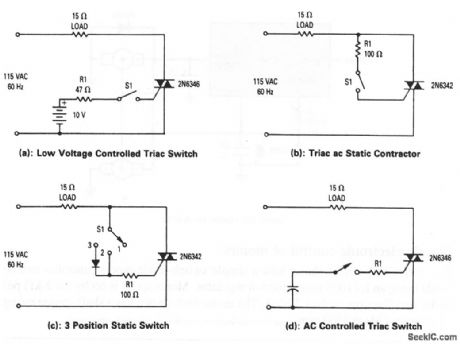
These circuits show triacs that are used to control a pure resistive load (of about 7 A) across an ac line. In Fig. 8-5A, gate current is supplied to the triac from the 10-V battery when S1 is closed. The triac tums on and remains on until S1 is opened. This cirquit switches at zero current, except for initial turn on, so S1 can be a very low-current switch (carring only triac gate current). The triac switch of Fig.8-5B has the same characteristics as Fig. 8-5A, except that the battery is eliminated. In the circuit of Fig. 8-5C, when S1 is in position 1, the triac receives no gate current and is nonconducting. With S1 in position 2, operation is the same as in Fig. 8-5B. With S1 in position 3, the triac receives gate current only on positive half-cycles, and power to the load is half-wave. Figure 8-5D shows ac control of the triac. (View)
View full Circuit Diagram | Comments | Reading(1704)
SPLIT_PHASE_CONTROL_WITH_BRAKING
Published:2009/7/7 4:55:00 Author:May
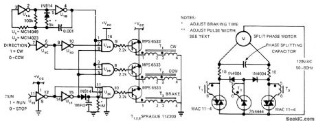
Use of CMOS logic to gate direction-controlling triacs and turn on SCR for braking provides lowcost switchless control of split-phase motor used In place of brush-type DC motor Aρplications include control of ball valves and other throtting functions in process control With shaft-position encoders, circuit generates feed-back information. Overshoot and other stability problems are easily controlled by strong braking function. CMOS logic provides complete noise immunity. Oscillator pulse width is adjusted with 1K resistor in series with 1N914, and brake duration is controlled by 1-megohm resistor at input of U2C. With values shown, brake is applied for about 1 s. Circuit works reliably on supply voltages of 5 to 15 V.-V. C. Gregory, Split-Phase Motor Control Accomplished with CMOS, EDN Magazine, 0ct. 5, 1974 p 65-67. (View)
View full Circuit Diagram | Comments | Reading(1529)
PREAMP_WITH_CLIPPING
Published:2009/7/21 22:01:00 Author:Jessie
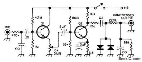
Increases speech intelligibility, particularly with SSB amateur stations Q1 and Q2 are HEP-54 Diodes are 1N456 or HEP-158.-Circuits,73 Magazine, Feb,1974.p100. (View)
View full Circuit Diagram | Comments | Reading(731)
STALLED_MOTOR_PROTECTION
Published:2009/7/7 4:42:00 Author:May
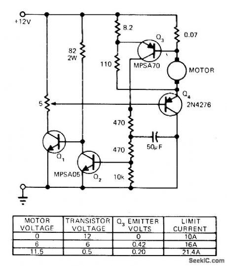
Modification of basic speed control circuit for small DC permanent-magnet motors provides maximum current limit under normal conditions and reduced current limit under stall conditions, to limit dissipation of series transistor Q4, to safe value. When motor stalls, motor voltage falls, reducing voltage and motor current required to turn on Q3 and thereby limiting stalled-motor current,-D. Zinder, Current Limit and Foldback for Small Motor Control, EDN Magazine. May 5, 1974, p 77 and 79. (View)
View full Circuit Diagram | Comments | Reading(2658)
24_VDC_PROPORTIONAL_SPEED_CONTROL
Published:2009/7/7 4:39:00 Author:May
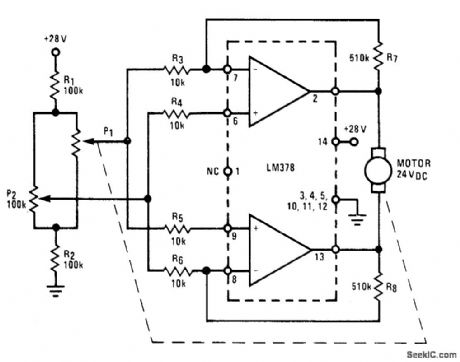
National LM378 amplifier IC is basis for low-cost proportional speed controller capable of furnishing 700 mA continuously for such applications as antenna rotors and motor-controlled valves. Proportional control results from error signal developed across Wheatstone bridge R1-R2-P1-P2. P1 is mechanically coupled to motor shaft as continuously variable feedback sensor. As motor turns, P1 tracks movement and error signal becomes smaller and smaller; system stops when error voltage reaches 0 V.- Audio Handbook, National Semiconductor, Santa Clara, CA, 1977, p 4-8-4-20. (View)
View full Circuit Diagram | Comments | Reading(2176)
TRANSISTOR_PROTECTION_IN_MONO
Published:2009/7/21 10:27:00 Author:Jessie
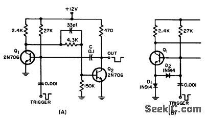
In typical transistor monostable mvbr (A), transient base-to-emitter voltage caused by discharging C often surpasses transistor rating. Two diodes alleviate trouble (B). Circuit produces width of 200 microsec.-J. S. Mikuckis, Base-Emitter Protection in Monostable Multivibrators, EEE, 12:9, p 63. (View)
View full Circuit Diagram | Comments | Reading(1141)
OVERLOAD_PROTECTION_WITH_TD
Published:2009/7/21 10:26:00 Author:Jessie
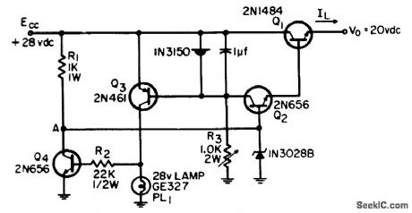
Tunnel diode-transistor level detector reduces load current of series voltage regulator to zero when preset limit is exceeded. Protective circuitry consists of TD1, PL1, R2, R3, Q3, and Q4.-G. E. Bloom, Overload Protection with a Tunnel Diode, EEE, 12:10, p 60 and 75. (View)
View full Circuit Diagram | Comments | Reading(754)
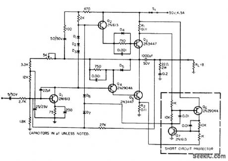
COMPLETE_GTO_PROTECTION_FOR_D_C_SUPPLY
Published:2009/7/21 10:24:00 Author:Jessie
Circuit includes required recycle pulse generator and Schmitt trigger for driving gate-turnoff scr (gto) that switches off d-c power supply within 30 microsec of over-load. Series regulator can deliver 125 V at 1 amp for input of 31 to 42 V. Overload trip point can be set anywhere between 0.75 and 1.2 amp. –W. C. Mosley, GTO Protection Circuitry for DC Supplies, EEE, 12:11, p 57-59. (View)
View full Circuit Diagram | Comments | Reading(1060)
SHORT_CIRCUITABLE_30_W_AUDIO_AMPLIFIER_
Published:2009/7/21 10:21:00 Author:Jessie
Utilizes practically entire supply voltage to produce usable power output, provides fail-safe overload protection, and stabilizes bias current. Any temporary overload or current surge will turn off drive to output stage. Circuit must be reset manually, by turning S1 off, removing cause of overload, and turning S1 on again. Circuit will limit peak current in output transistors Q3 and Q5 to about 5 amp.-W. O. Hamlin, Transformer. less Amplifier with Overload Protection, EEE, 12:9, p 42-44. (View)
View full Circuit Diagram | Comments | Reading(1183)
| Pages:127/312 At 20121122123124125126127128129130131132133134135136137138139140Under 20 |
Circuit Categories
power supply circuit
Amplifier Circuit
Basic Circuit
LED and Light Circuit
Sensor Circuit
Signal Processing
Electrical Equipment Circuit
Control Circuit
Remote Control Circuit
A/D-D/A Converter Circuit
Audio Circuit
Measuring and Test Circuit
Communication Circuit
Computer-Related Circuit
555 Circuit
Automotive Circuit
Repairing Circuit