
Control Circuit
Index 126
SOUND_ACTIVATED_TAPE_SWITCH
Published:2009/7/7 20:38:00 Author:May
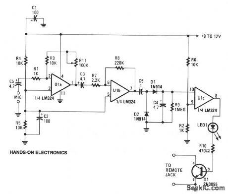
This circuit can cause a cassette recorder to automatically turn on and record when a sound or noise is present. Another use, is when the sound-activated switch is used to turn on a cassette player so that it operates as a burglar-alarm detector and sounder. Op amps U1a and U1b are connected in tandem to amplify the sounds picked up by the detector's mike. The amplified audio voltage, output at pin 7 of U1b, is fed to a voltage-doubler circuit, consisting of D1 and D2. The elevated voltage from the doubler circuit is input to the positive input of op amp U1c, which is operating as a simple comparator circuit. The other input of Ulc is connected to a voltage divider that sets the switching point for the dc signal voltage, to turn on when the signal level is greater than about 1.5 V. As the comparator switches on, its output at pin 8 becomes positive and supplies a forward bias to turn on D3 and Q1, which in turn, starts the recorder. The rc combination of C4/R9 sets the cassette's run time after the input sound has ceased, preventing the recorder from chopping-up or turning-off between closely spaced sounds or words picked up by the mike. The delay time is roughly 6 to 8 seconds. R11 sets the circuit's gain. Connect a low-impedance cassette mike to the amplifier's input, and connect the output of Q1 to the cassette's remote input or to the internal input and set the recorder to the record position. Talk and adjust the amplifier's gain with R11 for the desired sensitivity. (View)
View full Circuit Diagram | Comments | Reading(2680)
SOUND_ACTIVATED_SWITCH
Published:2009/7/7 20:33:00 Author:May

A sensitive electret microphone picks up the sound and feeds the signal to a two-stage amplifter circuit, consisting of U1a and U1b. The amplified output of U1b is fed to a voltage-doubler circuit (comprised of D1, D2, C4, and C5). The output of the doubler is input to the gate of Q1. When the dc voltage reaches the gate's threshold level, Q1 switches on, starting the recorder. Resistor R6 sets the circuit's sensitivity and should be experimented with to obtain the optimum adjustment. (View)
View full Circuit Diagram | Comments | Reading(0)
ARC_PROTECTION_CIRCUIT
Published:2009/7/21 10:58:00 Author:Jessie
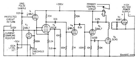
Circuit ignores desired peak pulse currents by sensing their coincidence with drive pulse, but fires trigger thyratton V6 and V7 in absence of drive pulse, to make thyratrons discharge power supply before breakdown and flashover of high-voltage electron device under test.-D. D. Mawhinney, Latest Thing in Arc-Protection Circuits, Electronics, 36:8, p 54-55. (View)
View full Circuit Diagram | Comments | Reading(834)
LIFESAVER
Published:2009/7/21 10:55:00 Author:Jessie
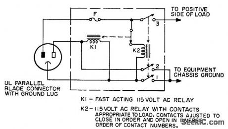
Used with transformerless line-operated equipment to minimize possibility of chassis being hot. Relays are so arranged that they automatically search for proper relationship of voltages between hot, neutral and ground terminals before power is applied to equipment. Only limitation is failure to protect against rare fault in which both neutral and conduit ground are at line potential with respect to earth ground.-R. E. Pafenberg, Lifesaver Circuit, EEE, 10:7, p 26-27. (View)
View full Circuit Diagram | Comments | Reading(740)
ANALOG_SWITCH
Published:2009/7/7 20:07:00 Author:May
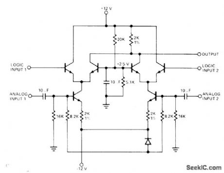
Circuit using Signetics 511 transistor array provides digital selection of either of two analog signals. When logic input at left is zero, signal at analog input 1 goes to output and other analog input signal is rejected. Similarly, when logic 0 is applied to logic input 2, analog input 2 goes to output. Eight-channel analog multiplex switch can be formed by combining four 511 analog switches with Signetics 8250 binary-to-octal decoder. Analog signals up to 200 kHz are switched without amplitude degradation.- Signetics Analog Data Manual, Signetics, Sunnyvale, CA, 1977, p 753-754. (View)
View full Circuit Diagram | Comments | Reading(0)
OVERLOAD_PROTECTION_FOR_REGULATED_POWER_SUPPLY
Published:2009/7/21 10:54:00 Author:Jessie
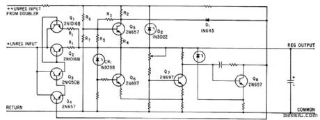
When rated load current is exceeded in series-regulated power supply, D1 conducts and collector voltage of Q1 acts as clamp to prevent further increase in load current. At short-circuit, load current is only fraction of full value.-K. L. Burfeindt, Over-load Protection Without High Power Dissipation, Electronics, 36:13, p 36-37. (View)
View full Circuit Diagram | Comments | Reading(814)
THYRATRON_PROTECTION_IN_HIGH_VOLTAGE_SWITCH
Published:2009/7/21 10:31:00 Author:Jessie
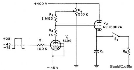
C1 is charged to some value up to 400 V, then discharged into load R5 by gas tube represented by S1. V2 acts as cathode follower to charge C1 as long as V1 does not conduct. When operation of S1 is desired, V2 is turned off by turning on V1 long enough for S1 to operate and recover, using square-wave input pulse. Circuit action prevents destruction of thyratron switch and load without sacrificing pulse rate. Tubes need separate filament transformers.-Voltage Controlled High Voltage Switch, Electronic Circuit Design Handbook, Mactier Pub. Corp., N.Y., 1965, p 233. (View)
View full Circuit Diagram | Comments | Reading(987)
BASIC_GTO_FOR_POWER_SUPPLY_OVERLOADS
Published:2009/7/21 10:30:00 Author:Jessie

Gate-turnoff scr (GTO) provides superior overload protection for d-c power supplies. Chief advantages are elimination of tum-on current surges, switching off within 30 microsec of overload, automatic load sensing, and reset, and no appreciable effect on power supply efficiency.-W. C. Mosley, GTO Protection Circuitry for DC Supplies, EEE, 12:11, p 57-59. (View)
View full Circuit Diagram | Comments | Reading(1239)
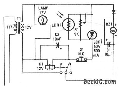
CONSTANT_BRIGHTNESS_CONTROL
Published:2009/7/7 9:59:00 Author:May

An automatic control maintains a lamp at a constant brightness over a wide range of supply voltages. This circuit utilizes the consistency of photodiode response to control the phase angle of power line voltage applied to the lamp and can vary the power between that available and ≈ 30% of available. This provides a candlepower range from 100% to less than 10% of nominal lamp output. The 100-μH choke, resistor, and capacitors form an rlc filter network that is used to eliminate conducted RFI. (View)
View full Circuit Diagram | Comments | Reading(875)
OVERVOLTAGE_INDICATOR
Published:2009/7/21 10:28:00 Author:Jessie
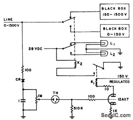
Routes line voltage automatically to black box designed to handle it. Potentiometer is set so neon lamp TH fires at 152 V. This applies high negative voltage to grid of tube, deenergizing relays K1 and K2 so line voltage is applied to upper black box. This condition also exists when system is first connected to line. After tube is warmed up, it switches to low-voltage box if line is below 152 V. Rectifier CR is any 2,000-V low-current rectifier, such as Sarkes Tarzian 126-100-H-Q. NE68 glow lamp TH must be in lightproof box; NE2 can be used only if suitably aged.-Overvoltage Indicator, Electronic Circuit Design Handbook, Mactier Pub. Corp., N.Y., 1965, p 124. (View)
View full Circuit Diagram | Comments | Reading(738)
PULSE_WIDTH_MODULATION_LAMP_BRIGHTNESS_CONTROLLER
Published:2009/7/7 9:57:00 Author:May
At half brightness, the lamp current is pulsed on and off (Fig. 50-12b) by the voltage developed across the resistor and capacitor at the current-sense output. Lamp current is sensed by the current-sense out-put. A simple pulse-width modulation lamp-brightness control circuit can also be built with the device. When the device powers up, the sense output is low, pulling the comparator output and the on input low, and turning the FET switch on. When the switch is on, current from the sense output charges the capaci-tor in the rc timing network to the 200-mV comparator threshold voltage. The comparator trips, turning the switch off. The charge then leaks off the capacitor, its voltage drops below 100 mV, and the FET is again turned on. The average current through the load is basically a function of the resistor value. The pulse-width modulation frequency on the other hand, is a function of the capacitor value. (View)
View full Circuit Diagram | Comments | Reading(832)
PHASE_CONTROL_1
Published:2009/7/7 9:53:00 Author:May
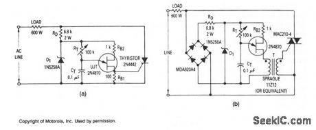
The most elementary application is a half-wave control circuit. The thyristor is acting both as a power control device and as a rectifier, providing variable power to the load during the positive half cycle and no power to the load during the negative half cycle. The circuit is designed to be a two terminal control which can be inserted in place of a switch. If full-wave power is desired as the upper extreme of this control, a switch can be added which will short circuit the SCR when RT is turned to its maximum power position. Full-wave control might be realized by the addition of a bridge rectifter, a pulse transformer, and by chang-ing the thyristor from an SCR to a TRIAC, shown in Fig 50-9b. In this circuit,RB1 is not necessary since the pulse transformer isolates the thyristor gate from the steady-state UJT current. Occasionally, a circuit is required to provide constant output voltage regardless of line voltage changes. Adding potentiorneter P1 to the circuits will provide an approximate solution to this problem. The potentiometer is adjusted to provide reasonably constant output over the desired range of line voltage. (View)
View full Circuit Diagram | Comments | Reading(1121)
TRIAC_LIGHT_DIMMER
Published:2009/7/7 9:48:00 Author:May
View full Circuit Diagram | Comments | Reading(174)
PHASE_CONTROL
Published:2009/7/7 9:48:00 Author:May
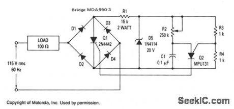
This circuit uses a PUT for phases control of an SCR. The relaxation oscillator formed by Q2 provides conduction control of Q1 from 1 to 7.8 ms or 21.6° to 168.5°. This constitutes control of over 97% of the power available to the load. Only one SCR is needed to provide phase control for both the positive and negative portion of the sine wave by putting the SCR across the bridge-composed of diodes D1 through D4. (View)
View full Circuit Diagram | Comments | Reading(1115)
RF_ACTUATED_RELAY
Published:2009/7/7 8:08:00 Author:May
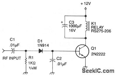
Automatic antenna switching or rf power indi-cation can be achieved with this circuit. Relay will key with less than 150 mW drive on 2 m. (View)
View full Circuit Diagram | Comments | Reading(1773)
RECEIVER_SIGNAL_ALARM
Published:2009/7/7 8:06:00 Author:May
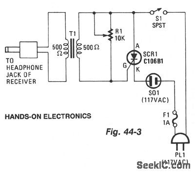
View full Circuit Diagram | Comments | Reading(756)
HALL_EFFECT_SWITCHES
Published:2009/7/7 7:31:00 Author:May

Hall-effect switches have several advantages over mechanical and optically coupled switches. They're insensitive to environmental light and dirt, they don't bind, and they don't sustain mechanical wear. Their major drawback is that they require three wires per device. The circuit shown, however, reduces this wire count to N + 1 wires for N devices.Amplifier IC1A is configured as a current-to-voltage converter. It senses the sensor assembly's out-put current. When the Hall-effect switch is actuated, the sensor's output current increases to twice its quiescent value. Amplifier IC1B, configured as a comparator, detects this increase. The comparator's out-put decreases when the Hall-effect switch turns on.The circuit also contains a fault-detection function. If any sensor output wire is open, its correspond-ing LED will turn on. If the power-supply line opens, several LEDs will turn on. A short circuit will also turn an LED on. Every time an LED turns on, Q1 turns on and the alarm relay is actuated. (View)
View full Circuit Diagram | Comments | Reading(3719)
SECURITY_DOOR_AJAR_ALARM
Published:2009/7/7 7:27:00 Author:May
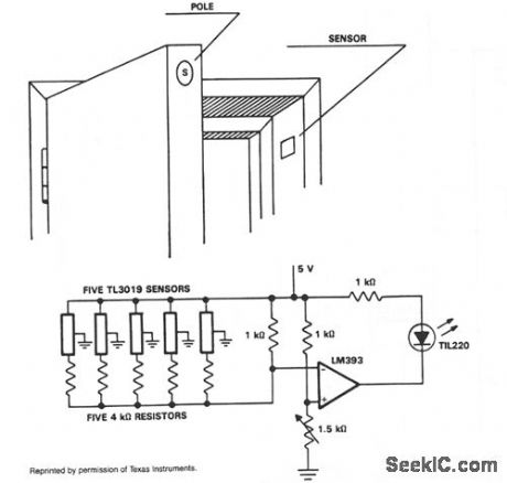
In operation, the TL3019 device will activate, or become low, when a south pole of a magnet comes near the chip face of the device. The example shows five doors. Each door has a magnet embedded in its edge with the south pole facing the outer surface. At the point where the magnet is positioned with the door closed, a TL3019 sensor is placed in the door jamb. With the door closed, the Hall devices will be in a logic low state. This design has five doors and uses five TL3019 devices. Each TL3019 has a 4-KΩ resistor in series and all door sensor and resistor sets are in parallel and connected to the inverting input of an LM393 comparator. With all doors closed, the effective resistance will be about 800 0 and produce 2.2 V at the inverting input. The noninverting input goes to a voltage divider network which sets the reference voltage. The 1.5-KΩ potentiometer is adjusted so the indicator goes out with all doors closed. This will cause 2.35 V to appear at the noninverting input of the comparator. When a door opens, the voltage at the inverting input will go to 2.5 V which is greater than VREF, and the LED will light. A large number of doors and windows can be monitored with this type of circuit. Also, it could be expanded to add an audible alarm in addition to the visual LED. (View)
View full Circuit Diagram | Comments | Reading(1080)
SCR_SMOKE_ALARM
Published:2009/7/7 7:15:00 Author:May
View full Circuit Diagram | Comments | Reading(712)
POWER_TRANSFORMER_SWITCHING_RELAY_SENSES_LINE_VOLTAGE
Published:2009/7/21 10:04:00 Author:Jessie
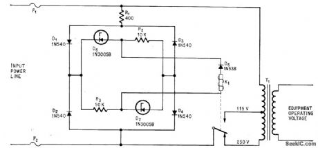
For 230-V line voltage, zener diodes back-bias D5, preventing energization of relay. For 115 V, diode conducts and relay closes, connecting line to 115-V tap of transformer. –L. K. Moyer, Circuit Always Applies Correct Operating Voltage, Electronics, 37:25, p 77. (View)
View full Circuit Diagram | Comments | Reading(940)
| Pages:126/312 At 20121122123124125126127128129130131132133134135136137138139140Under 20 |
Circuit Categories
power supply circuit
Amplifier Circuit
Basic Circuit
LED and Light Circuit
Sensor Circuit
Signal Processing
Electrical Equipment Circuit
Control Circuit
Remote Control Circuit
A/D-D/A Converter Circuit
Audio Circuit
Measuring and Test Circuit
Communication Circuit
Computer-Related Circuit
555 Circuit
Automotive Circuit
Repairing Circuit