
Control Circuit
Index 124
Automatic_level_control_circuit
Published:2009/7/21 3:17:00 Author:Jessie
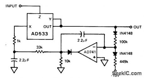
Automatic level control circuit. The AD533 is set up in the divide mode. Its output is rectified and compared with the power supply derived - 15volt reference. The net current is integrated by the AD741 and fed into the denominator input el the AD533, maintaining the level of the output at the AC average value programmed by the feedback circuitry, 7 volts in this case (courtesy Analog Devices, Inc.). (View)
View full Circuit Diagram | Comments | Reading(1000)
BURST_POWER_CONTROL
Published:2009/7/8 4:15:00 Author:May

Industrial applications sometimes require that power be only briefly applied to a load following the closure of a switch, such as a microswitch or foot switch. The load could be a heating element for use in sealing plastic bags, a dc motor that is indexed or stepped with each application of power, or a dc solenoid which is to be energized for a brief time-for example, a staple gun.
The phase angle at which the SCR triggers on is determined by the charging rate of C2 through R7 and potentiometer R8. When the breakover voltage of the gate triggering device, a silicon unilateral switch, is reached, the SCR turns on. The average dc voltage to the load is determined by the setting of R8.
(View)
View full Circuit Diagram | Comments | Reading(1268)
SIMPLE_LOW_COST_RF_SWITCH
Published:2009/7/8 4:13:00 Author:May
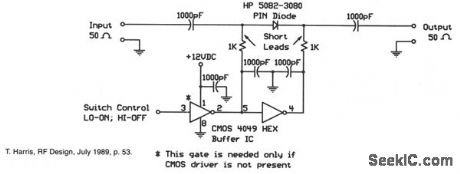
When the digital logic level at the control input is low, the PIN diode is forward-biased by the CMOS gates. The two 1-KΩ bias resistors limit this current to the PIN diode's safe forward current limit. In this state, the switch is on. When the control input is high, the diode is reverse-biased and the switch is off.This switch is well-suited for electronically steered antenna arrays, multiple path switching, and other applications requiring small, low-cost rf switches. This particular design was used in a four-pole rotary switch for a Doppler-shift radio direction-finder operating at 144 MHz.
(View)
View full Circuit Diagram | Comments | Reading(955)
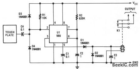
TOUCH_SWITCH_1
Published:2009/7/8 3:58:00 Author:May
View full Circuit Diagram | Comments | Reading(1462)
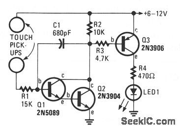
TOUCH_SWITCH
Published:2009/7/8 3:54:00 Author:May
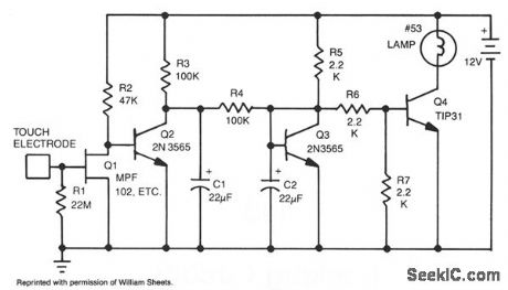
This touch-actuated switch stays on as long as you keep your finger on the touch plate. R1 sets the input impedance to a high 22 M Ω. Q1 picks up stray signals coupled through your body to the touch plate and amplifies them to tum on Q2, which tums on lamp drivers Q3 and Q4. Lamp I1 is any small 12-V lamp, such as a No. 53-12 V 120 mA. R4 and C1 add a small amount of hysteresis (delay) to keep the light from constantly flickering. A relay can be used for I1. (View)
View full Circuit Diagram | Comments | Reading(0)
LINE_HUM_TOUCH_SWITCH
Published:2009/7/8 3:47:00 Author:May
The monostable period is set for about 1 second, as is the usual case. The induced line hum comes through C2, providing a continuous string of trigger pulses. The output becomes low for about 10 ms per second as the monostable times out and then retriggers. Diode Dl and capacitor C3 buffer the relay so it doesn't chatter on those 10-ms pulses. Resistor R2 sets the sensitivity.The relay energizes when the plate is touched and de-energizes, up to one second after the finger is removed. The delay is a function of when the monostable last retriggered. (View)
View full Circuit Diagram | Comments | Reading(1038)
TOUCH_ON_OFF_ELECTRONIC_SWITCH
Published:2009/7/8 3:45:00 Author:May

Transistors Q1 and Q2 control latch Q3 and Q4 to switch on the lamp. A high resistance from touching the electrode biases Q1 or Q2 on, setting or resetting the latch. (View)
View full Circuit Diagram | Comments | Reading(906)
TWO_TERMINAL_TOUCH_SWITCH
Published:2009/7/8 3:43:00 Author:May
This circuit requires the bridging of two circuits to activate the electronic switch. That circuit does not require a 60-Hz field to operate and can be battery or ac powefed. The two-pickup terminals can be made from most any clean metal; they should be about the size of a penny. The input circuitry of the two-terminal touch switch is a high-gain Darlington amplifier that multiplies the small bridging current to a value of sufficient magnitude to turn on Q3, supplying power to LED1. If a quick on and off switching time is desired, the value of C1 should be very small; if a long on-time period is required, the value of C1 can be increased. (View)
View full Circuit Diagram | Comments | Reading(805)
DIGITAL_TOUCH_ON_OFF_SWITCH
Published:2009/7/8 3:41:00 Author:May
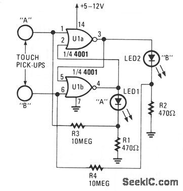
Only one LED can be on when the circuit is at rest. Which LED is illuminated is determined by the touch pick-up that last had human contact. Pickup terminal A controls the on condition of LED1, and terminal B controls the on condition of LED2. A 4001 quad two-input NOR gate is connected in an anti-bounce latching circuit that is activated by touching a pickup. (View)
View full Circuit Diagram | Comments | Reading(1049)
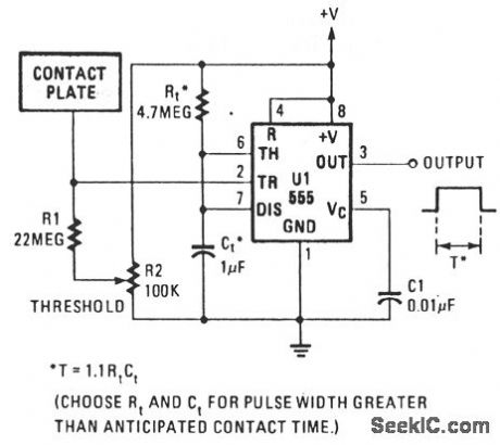
ANTICIPATING_CONTROLLER
Published:2009/7/8 3:23:00 Author:May
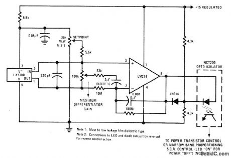
Circuit adds selected amount of phase Ieading signal to notmal amplified output of National LX5700 temperature sensorto compensate at least partially for sensing Iags. DC gain of LM216 opamp is set at t0 by 10-megohm and 100-megohm resistors to give opamp output of 1 V/°C. Output of opamp energizes optoisolator that feeds conventional temperature control system.-P. Lefferts, A New Interfacing Concept; the Monolithic Temperature Transducer, National Semiconductor, Santa Clara, CA, 1975, AN-132, p 7. (View)
View full Circuit Diagram | Comments | Reading(714)
0000033℃_CHOPPER_STABILIZED_OVEN_CONTROL
Published:2009/7/8 3:18:00 Author:May
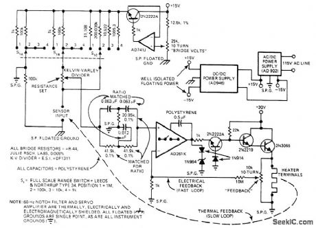
Uses chopper-stabilization techniques to provide ultimate in temperature control for laboratory oven. Multiranging bridge accommodates sensols from 10 ohms to 1 megohm, with Kelvin-Valley divider being used to dial sensor resistance control point directly to five digits. Use of floating power supply for bridge allows single-ended noninverting chopper-stabilized AD741J amplifier to take differential measurement and eliminates commonmode voltage elror. Passive 60-Hz notoh fittel eliminates pickup noise at input of AD261K amplifier which in turn feeds 2N2222A transistor driving Darlington pair that provides up to 30 V across heater of oven. Article also gives circuit of 30-V regulated supply required for output transistors.-J. Williams, Designer's Guide to: Tempelature Contlol, EDN Magazine, June 20, 1977, p 87-95.
(View)
View full Circuit Diagram | Comments | Reading(1079)
THREE_BAND_ACTIVE_TONE_CONTROL
Published:2009/7/8 3:17:00 Author:May
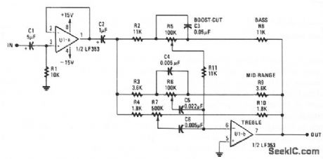
View full Circuit Diagram | Comments | Reading(3978)
IC_PREAMPLIFIER_TONE_CONTROL
Published:2009/7/8 3:12:00 Author:May
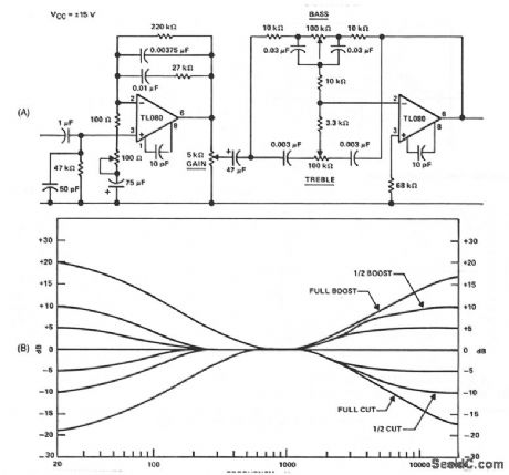
The circuit is a form of the so-called Americanized version of the Baxandall negative-feedback tone control. At very low frequencies, the reactance of the capacitor is large enough that they might be considered open circuits, and the gain is controlled by the bass potentiometer. At low to middle frequencies, the reactance of the 0.03-μF capacitors decreases at the rate of 6 dB/octave, and is in parallel with the 200-KΩ potentiometer; so the effective impedance is reduced correspondingly, thereby reducing the gain. This process continues until the 10-KΩ resistors, which are in series with the bass pot, become dominant and the gain levels off at unity. The action of treble circuit is smaller and becomes effective when the reactance of the 0.003- μF capacitors becomes minimal. This complete tone control is in the negative feedback loop of the TL080. Figure B shows the bass and treble tone control response. (View)
View full Circuit Diagram | Comments | Reading(4373)
0000075℃_BATH_CONTROL
Published:2009/7/8 3:03:00 Author:May
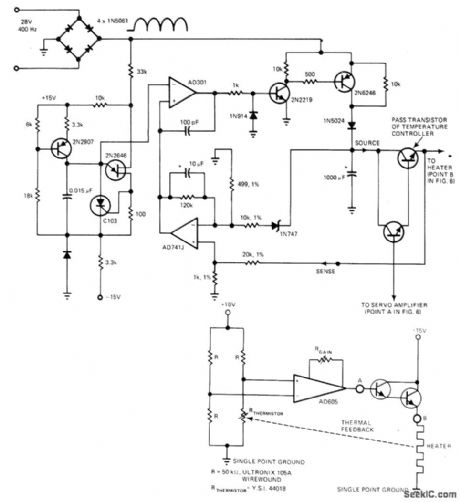
Will hold oven or bath at 37.5 ℃ with high stability. Bridge offset is sensed by AD605 instrumentation opamp having high common-mode rejection, low drift, and balanced inputs. Opamp drives Darlington pair providing current gain to heater. Pass transistor must dissipate all power not delivered to heater; to overcome this, large servo circuit is connected between points A and B to maintain constant 3 V across pass transistor regardless of heater power demands. Output of 741 opamp is compared with 400-Hz line-synchronized ramp by AD301A amplifier serving as pulse-width modulator that drives 2N2219-2N6246 transistor switch. Switch delivers phase-con-trolled power to 100-μF integrating capacitor and pass transistor of temperature controller.-J. Williams, Designer's Guide to: Temperature Control, EDNMagazine, June 20, 1977, p 87-95. (View)
View full Circuit Diagram | Comments | Reading(897)
ROOM_HEATER_CONTROL
Published:2009/7/8 1:57:00 Author:May
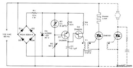
Use of phase control for triac provides gradual reduction in heater load current as desired temperature is approached, eliminating large overshoots. R2 is adjusted so al is of at desired temperature, turning Q2 off and preventing firing of triac. If temperature decreases, resistance of sensor RT increases and transistors initiate firing of triac.If RT continues to increase, C1 charges faster and triac is triggered earlier in each half-cycle, delivering more power to load. Dashed Iines indicate alternate connections for controlling motor with constant load such as blower motor. For cooling applications, interchange FIT and R2.- Circuit Applications for the Triac, Motorola, Phoenix, AZ, 1971, AN-466, p 9.
(View)
View full Circuit Diagram | Comments | Reading(1111)
THERMOCOUPLE_WITH_ZERO_VOLTAGE_SWITCH
Published:2009/7/8 1:55:00 Author:May
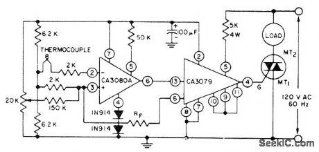
Differential input connection of RCA CA3080A operational transconductance amplifier is used with thernlocouple to drive CA3079 zero-voltage switch serving as trigger for triac handling AC load. Choose triac to match load being controlled. Supply voltage for opamps isnot criticaL.- Linear Integrated Circuits and MOS/FET's. RCA Solid State Division, Somerville, NJ, 1977, p 165-170.
(View)
View full Circuit Diagram | Comments | Reading(1435)
LOW_DISSIPATION_SWITCH
Published:2009/7/8 1:53:00 Author:May
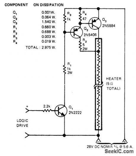
Logic-controlled power switch for 150-W instrument heater uses tap on heating element to force switch Q3, and driver Q2, into saturation and keep dissipation low. When input goes positive, Q1 turns on and drives Q2 and Q3 on. Collector current of Q2, and base drive of Q3 are determined by R2,. Voltage drop across R2 is proportional to supply voltage so drive for Q3 is at optimum level over wide voltage range,-M. Strange, Increase Electronic Power Switch Efficiency, EDN Magazine, Aug.20, 1975, p 78.
(View)
View full Circuit Diagram | Comments | Reading(798)
PHASE_FIRED_SCR_CONTROL
Published:2009/7/8 1:49:00 Author:May
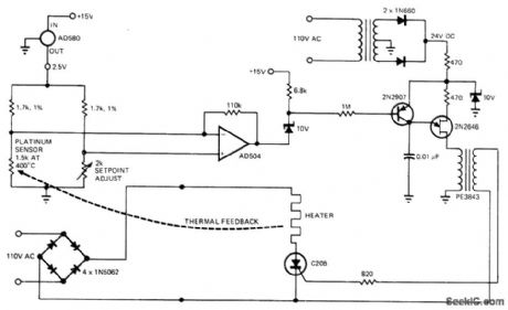
Can provide linear thermal control to 0.001℃ at high power with good efficiency. Band-gap voltage reference of AD580 IC temperature transducer furnishes power to bridge circuit, while platinum sensor provides sensing function, AD504 opamp amplifies bridge output for biasing 2N2907 transistor which in turn controis 60-Hz synchronized UJT oscillator that drives gate of SCR through isolation transformer. Biasing action makes SCR fire at different points on AC waveform as required for precise control of oven heater. Possibledrawback is RF noise generated because SCR chops in middle of wave-form,-J. Williams, Designer's Guide to: Temperature Control, EDNMagazine, June 20, 1977, p87-95. (View)
View full Circuit Diagram | Comments | Reading(871)
CRYSTAL_OVEN_CONTROL
Published:2009/7/8 1:47:00 Author:May
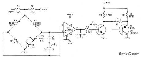
Unbalance voltage produced in thermistor bridge when temperature drops below set point is sensed by differential opamp that feeds buffer Q1 and power amplifier Q2, Power dissipated in Q2 and its load R11 heats oven. Thermistor R4 has nominal resistance of 3600 ohms at 50℃ (GE 1D53 or National Lead 1D053). Voltage divider R1-R2 reduces U1 input to safe Ievel and makes thermistor operate at low current, minimizing self-heating effects. All arms of thermistor bridge except R7 (vemier temperature ad justment) are in oven.-R. Silberstein, An Experimental Frequency Standard Using ICs, QST, Sept. 1974, p 14-21 and 167.
(View)
View full Circuit Diagram | Comments | Reading(820)
TIME_PROPORTIONAL_CONTROL
Published:2009/7/8 1:41:00 Author:May
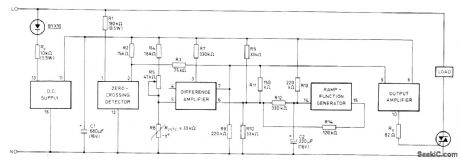
Provides synchronous ON/OFF switching of resistive load under control of temperature-sensitive bridge formed by R4, R5, and negative temperature coefficient thermistor R6 in one bridge branch, with R9 and R10 in other branch. All required function elements are included in Mullard TCA280A trigger module. Values shown are for triac requiring gate cuwent of 100 mA; for other triacs, values of Rd' Rg'and C1 may need to be changed. Proportional band can be adjusted by changing value of R12, Triac triggering coincides with zero crossings of AC line voltage.Repetition time of internally generated siwtooth is about 30 s and can be adiusted by changing C2.- TCA280A Trigger IC for Thy ristors and Triacs, Mullard, London, 1975, Technical Note 19, TP149O, p 10.
(View)
View full Circuit Diagram | Comments | Reading(973)
| Pages:124/312 At 20121122123124125126127128129130131132133134135136137138139140Under 20 |
Circuit Categories
power supply circuit
Amplifier Circuit
Basic Circuit
LED and Light Circuit
Sensor Circuit
Signal Processing
Electrical Equipment Circuit
Control Circuit
Remote Control Circuit
A/D-D/A Converter Circuit
Audio Circuit
Measuring and Test Circuit
Communication Circuit
Computer-Related Circuit
555 Circuit
Automotive Circuit
Repairing Circuit