
Control Circuit
Index 110
COHO_JITTER_MONITOR
Published:2009/7/17 3:01:00 Author:Jessie
Automatically monitors coherent oscillator frequency and provides visible indication of amount of jitter, as measure of mti system capability.-C. Clark, Checking Jitter in Moving Target Radar, Electronics, 32:29, p 56-58. (View)
View full Circuit Diagram | Comments | Reading(787)
TWO_TIMER_KEYER
Published:2009/7/11 4:00:00 Author:May
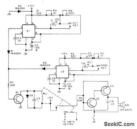
Characters are self-completing and fully adjustable as to speed and length of character. When dot key is closed, NE555 timer U1 becomes astable MVBR with speed determined by F1B and dot duration by RA Identical timer U2 provides longercharacter lengths for dashes. All diodes are 1N4004 or equivalent 400 V PIV at 1 A. Q1 and Q2 are 2N2222, Q3 is 2N5964, and RL1 is 12-V reed relay. Capacitor values are in microfarads. All pots are linear. Power is not regulated.-A.Ring, Build the World's Simplest Keyer, 73 Magazine, May 1977, p 46-47. (View)
View full Circuit Diagram | Comments | Reading(883)
VFO_CONTROL_TO_±1Hz
Published:2009/7/11 3:52:00 Author:May

Usea in coherent CW radio station to hold frequency of variable-frequency oseillator constant at 3550 kHz within 1 Hz so 12-WPM signal can be handled in bandwidth of only 9 Hz for greatly improved signalto-noise ratio. Sample of VFO output, squared by Q1 and U1 goes to U2 for mixing with 3500,000-kHz harmonic signal from 500-kHz froquency standard,to produce 50-kHz signal ±unclesired driftfor mixing in U3A with 50,000-kHz signal from standard .If there is difference in frequency,U3A generates control voltage proportional to amount of difference,applied to varactor tuning diode to pull VFO back to 3550.000 kHz. Same process occurs in receive offset chain, except that standard frequency in U3B is such that receiver will be 1 kHz away from desired 3550.000 kHz and produce desired 1-kHz audio output.-A. Weiss, Coherent C.W.-the C.W. of the Future, CQ, June 1977, p 24-30.
(View)
View full Circuit Diagram | Comments | Reading(1059)
KEYEB_WITH_IP_CONTROL
Published:2009/7/11 3:51:00 Author:May
Provides automatic control of TR relay for break-in operation,74221 TTL retriggerable mono MVBR forms dots or dashes with paddle selecting side of IC that puts out pulse.Half of A2(74123 dual retriggerable mono MVBR with clear)makesspaces between dots or dashes Remaining half of A2 acts with A3b and A3c as TR switch.-B,Voight,The TTL One Shot,73 Magazine.Feb,1977,p 56-58. (View)
View full Circuit Diagram | Comments | Reading(1436)
0_60_WPM_KEYER
Published:2009/7/11 3:51:00 Author:May
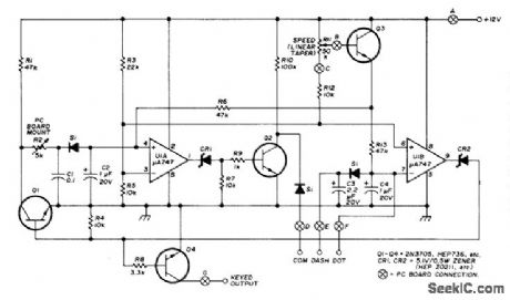
Uses μA747 (pair of μA741Cs in 10-pin TO-5 package). R2 adjusts relative length of first two dits to provide even spacing. Dot-dash ratio is set by C3 and C4, with C4 fordotand both in parallel fordash. Collector of C4 provides for keying positive voltage (20 V or less) to ground. Keying transistorwill handle up to 50 mA without heatsink. Characters are self-completing. Used with low-power transceiven-H. F, Batie, Introducing the Argomate, Ham Radio, April 1974, p 26-33. (View)
View full Circuit Diagram | Comments | Reading(729)
Bistable_switch_using_two_SUS_devices
Published:2009/7/17 2:45:00 Author:Jessie
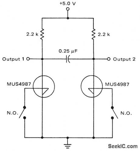
Bistable (memory) switch using two SUS devices. The mechanical switches can be replaced with other solid-state devices or negative-going pulses referenced to the supply line (courtesy Motorola Semiconductor Products Inc.). (View)
View full Circuit Diagram | Comments | Reading(1093)
DPDT_FET_switch
Published:2009/7/17 2:43:00 Author:Jessie
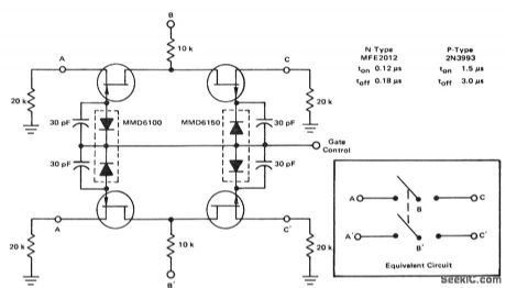
DPDT FET switch(courtesy Motorola Semiconductor Products Inc.). (View)
View full Circuit Diagram | Comments | Reading(1139)
FAILURE_MONITOR
Published:2009/7/17 2:38:00 Author:Jessie
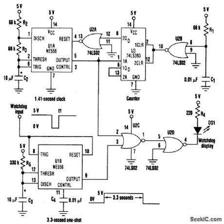
Some time ago, a situation arose in which a watchdog timer was needed to monitor an embedded computer. The computer in question required approximately 2 1/2 minutes to boot up and run the application software, so a monitor circuit was created that could wait 3 minutes before indicating failure. U1A, U2A, U2B, and U3 form a 3-minute timer. U1A operates as a free-running oscillator with a period of 1.41 s. The square-wave pulses are counted by U3, which generates an oscillator reset via U2A that effectively stops the clock. During the 3-minute interval, U2C and U2D send the oscillator signal to DS1, causing the indicator to flash. This flashing shows that the equipment is in its power-up cycle. When the reset occurs, the output of U1A is held low. U2B is a power-up reset for the counter. After 3 minutes, the indicator will come on continuously unless the watchdog input signal is present. U1B is configured as a 3.3-s-duration one-shot. When the watchdog input is pulsed low, the output switches high and keeps the LED from turning on. If the next pulse is not received in at least 3.3 s, the output will remain low. As a result, the LED will turn on, indicating failure. Should the watchdog input begin pulsing prior to the 3-minute timer, the watchdog will take precedence and turn off the flashing LED.What happens if the watchdog circuit fails? One of the characteristics of the NE556 timer is the inability to fully discharge the timing capacitor if the timer is retriggered prior to finishing a timing cycle. Applying a 10-Hz, 100-ms-wide pulsed input to the watchdog causes the capacitor charge to accumulate for approximately 8 s. This results in a 100-ms heartbeat flash of the LED every 8 s, which indicates that the circuit is still alive and that the LED hasn't burned out. The watchdog input is generated by an I/O line of the computer. Depending on the I/O board's design, the signal might need to be inverted to allow the watchdog input to remain normally high. (View)
View full Circuit Diagram | Comments | Reading(953)
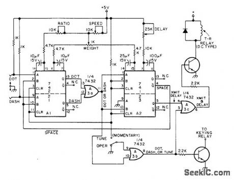
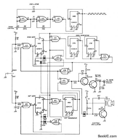
KEYER_SPEED_CONTROL
Published:2009/7/11 3:27:00 Author:May
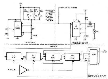
Electronic time base provides direct readout of keyer speed for 5 to 40 WPM in increments of 5 WPM by noting positions of three speed-control switches. Vemier adjustment pot R1 can be used for continuous speed adjustment if desired. Analog frequency meter provides alternate direct indication of keyer speed on milliammeter that can be call.brated in words per minute. Frequency of NE555 oscillator is 100 times keyer speed. Keyer clock is obtained by dividing oscillator speed by 120; thus, for 24 WPM oscillator runs at 2400 Hz which can be read easily on digital counter.Time-base divider would supply 20-Hz clock frequency for 24-WPM keying.-G. Jones, Calibrated Electronic Keyer Time Base, Ham Radio, Aug. 1975, p 39-41. (View)
View full Circuit Diagram | Comments | Reading(746)
REMOTE-CONTROLLED_SWITCHER
Published:2009/7/11 3:27:00 Author:May
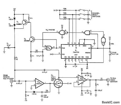

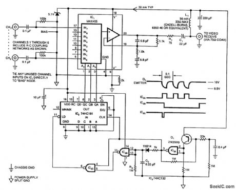
The interface end of Fig. 96-2(a)'s circuit deliver 10 V down the cable, pulses the supply voltage to transmit channel-change commands, and buffers the received video signal.The multiplexer circuit in Fig. 96-2(a) receives power and control signals over the coaxial cable, while driving the cable with the currently selected video signal.The interface circuit (Fig. 96-2(b)) delivers 10 V to the cable and pulses the supply voltage to select one of 8 channels. When the send button is depressed, a digital burst of 1.2 V amplitude (negative) is superimposed on the 12-V line (as a voltage drop). This does not affect the video signal. The multiplexer circuit (Fig. 96-2(c)) consists of a multiplexer and an amplifier. The multiplexer is a Maxim MAX455. The digital code on the supply line is picked off by A1, IC3A, and interfaced to counter IC2, which drives the multiplexer to select the desired video channel. (View)
View full Circuit Diagram | Comments | Reading(1113)
CMOS_KEYER_2
Published:2009/7/11 3:22:00 Author:May
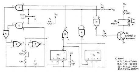
Gives variable speed, automatic spacing, and self-completing dots and dashes.Gates C, B, and Aform gated MVBR Dot paddle initiates dot by making output of gate D go low, while gate E goes low for dash. Character-shaping section (gates G, H, and F with JK flip-flops FF1 and FF2 takes square pulses from pin 3 of MVBR gate B and gives perfectly spaced dots and dashes. FF1 divides clock pulses by 2, making dot equal to one complete period of MVBR. FF2 divides output of FF1 by 2, and outputs of both flip-flops are logically ORed to provide dashes. K1 is SPST reed relay. Supply can be 9-V battery.-T. R. Crawford, A Low-Power Cosmos Electronic Keyer in Two Versions, CQ, Nov. 1975, p 17-24. (View)
View full Circuit Diagram | Comments | Reading(1062)
REMOTE_SELECTION_VIDEO_SWITCH
Published:2009/7/11 3:21:00 Author:May
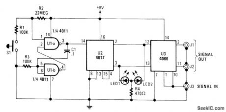
The A/B Switch circuit consists of three ICs and a handful of resistors. Two gates from a 4011 quad 2-input NAND gate (U1A and U1B) are configured as a monostable multivibrator that, when switch S1 is pressed, triggers a 4017 decade counter/divider, which has been set to recycle after a count of two. The outputs of U2 at pins 2 and 3 are fed to the control inputs of U3 (a 4066 quad bilateral syritch) at pins 12 and 13. Depending on which control input is high, either the J1 or J2 output is selected.With a little modification, the switch could be set to trigger at a set rate (automatically). With the addition of another 4066, it could have as many as 8 channels. One possible application would be in a security surveillance system. (View)
View full Circuit Diagram | Comments | Reading(2107)
UNDERVOLTAGE_DISCONNECT_SWITCH
Published:2009/7/17 2:32:00 Author:Jessie
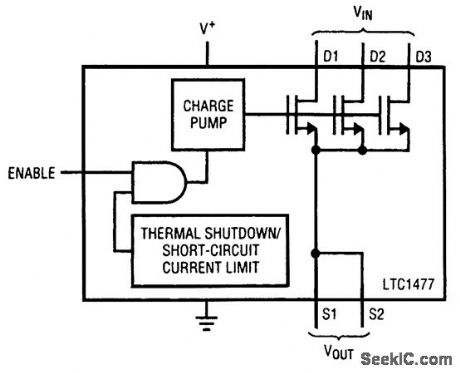
In an effort to conserve energy, simple shutdown schemes are incorporated into many battery-operated circuits. Not all circuits lend themselves to direct control, however. Instead, the supply must be turned off by a switch. The LTC1477 high-side switch is designed for this purpose and includes short-circuit current limiting and thermal shutdown to guard against faulty loads. The figure shows the LTC1477 and LTC699 conjoined in an undervoltage disconnect application. The LTC699 microprocessor supervisor disables the LTC1477; hence, the load is disabled whenever the input voltage falls below 4.65 V. An external logic signal applied to the gate of Q1 can also disable the LTC1477. When enabled, the LTC1477 output ramps over a period of approximately 1 ms, thereby limiting the peak current in the load capacitor to 500 mA. This prevents glitches on the 5-V source line that might otherwise affect adjacent loads. (View)
View full Circuit Diagram | Comments | Reading(926)
RECORDED_CODE_KEYER
Published:2009/7/11 3:12:00 Author:May
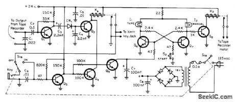
CW message recorded on cassette tape with keyed tone generato r is played back for keying transmitter with frequently repeated messages. Transmitted signal is essentially perfect reproduction of recording. Automatic transmission can be stopped at any point by tapping hand key; this deactivates tape recorder for manual keying of transmitter. All transistors are 2N2222 or equivalent BCY58. Use 24-V reed relays with 1K coil resistance. Pilot lamps are 24 V rated up to 3 W.CR1 is silicon diode. Whenever recorder emits beep, positive signal appears at base of Q2, making it conduct and activate K1 whose contacts go to key jack of transmitter.-A. Day, An Audio Tape-Controlled CW Keyer, CQ, Nov. 1971, p 31-32. (View)
View full Circuit Diagram | Comments | Reading(900)
CMOS_KEYER_1
Published:2009/7/11 3:00:00 Author:May

Features include self-completing dots and dashes, dot and dash memofies, iambic operation, dot and dash insertion, and automatic character spacing, all achieved with low-power CM0S digital devices that are compatible with low-power (QRP) transceiver operation, as with Heathkit HW-7 transceiver. Will operate directly from a-15 V batteries of QRP transceiver, without regulation.-G. Hinkle, The aRP Accu-Keyer, 73 Magazine, Aug. 1975, p 58-60. (View)
View full Circuit Diagram | Comments | Reading(2023)
KEYER_WITH_DOT_MEMORY
Published:2009/7/11 2:52:00 Author:May
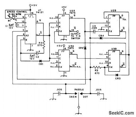
Features include self-completing characters, exact timing of characters, and dot memory. Timing circuit uses 74121 mono MVBR U1, serving dot gen-erator and output stage U2A, dot memory U2B, and dash generator U3A-U3B. U2 and U3 are 7473 dual JK flip-flops. Length of timing pulse is iletermined by R1-G1, with R1 controlling speed of keyer. Pulse-width stability at all speeds is better than 5% between first and all following pulses. Dot memory U2B allows keying of dot at any time, even if dash has not yet been completed. Dot is held in memory and keyed out automatically after dash. Diodes are 1N914.-J. H. Fox, An Integrated Keyer/TR Switch, QST, Jan, 1975, p 15-20. (View)
View full Circuit Diagram | Comments | Reading(1782)
CMOS_KEYER
Published:2009/7/11 2:43:00 Author:May
Draws only 0.4 mA on standby and 2 mA with key down if supply is 10 V. Will work properly with 4 to 15 V. Features include self-completing dots, dashes, and spaces, along with sidetone generator and built-in transmitter keying circuit. Ratio of dashes to dots is 3 : 1, and space has same duration as dot. Time base of keyer is generated by N0R gates U2C and U2D connected as class A MVBR. Frequency of oscillator is inversely linear with setting of R1.Inverter U3D buffers oscillator and squares its output. Flip-flop U6B divides frequency by2 and provides clock source with perfect 50% duty cycle. Once enabled, gates ensure completion along with following space. Article gives power supply circuit operating from AC line and 12-V battery.-J. W. Pollock, COSMOS IC Electronic Keyer, Ham Radio, June 1974, p 6-10. (View)
View full Circuit Diagram | Comments | Reading(1049)
HIGH_PERFORMANCE_VIDEO_MIXER
Published:2009/7/11 2:22:00 Author:May
This circuit mixes H synch. V synch. and actual video. T2 mixes the synch, while T1 serves as an emitter-follower. Bandwidths of up to 25 MHz are typical for this circuit. (View)
View full Circuit Diagram | Comments | Reading(1584)
PWM_MODEL_RAILROAD_CONTROLLER
Published:2009/7/17 3:28:00 Author:Jessie
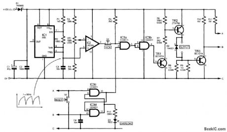
The PWM model train controller shown offers results that are far superior to those of a traditional rheostat-type model train controller and provides better fine control of train speeds. A 555 timer chip (IC1) is configured as a free-running oscillator operating at 80 kHz. The exponential ramp waveform generated across capacitor C3 feeds a comparator (IC2), whose threshold reference is set by logarithmic potentiometer VR1. The output of comparator IC2 is inverted by IC3a and IC3b and it drives the output stage, which comprises transistors TR1 and TR2; the latter can handle 2 A and dissipate 1 W, which is more than adequate for a saturated switch operation. Diode D2 protects against back BMP in the train motor. Short-circuit protection is provided with a 0.5-Ω series sense resistor (R8/R9). Transistor TR3 switches on when the current flowing reaches approximately 1.2 A. This sets the out-put of an S-R flip-flop (IC3c/lC3d) low. LED D3 illuminates to indicate a fault, and TR1 is disabled by the inverters. Capacitor C4 introduces a short time period across TR3 to prevent the cutout from triggering falsely. Push-switch S1 is a kick button. Pressing this causes a short, higher-voltage burst to be applied to reluctant motors. (View)
View full Circuit Diagram | Comments | Reading(7355)
Long_term_precision_integrator_for_such_applications_as_pollution_control
Published:2009/7/17 3:06:00 Author:Jessie
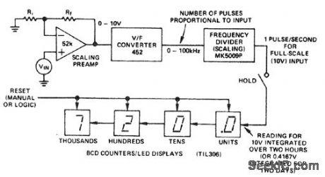
Long-term precision integrator for such applications as pollution control. The analog signal is applied to precision amplifier model 52K, then to the V/F converter input. Model 452's output is connected to a high capacity counter and display operating as a totalizer. The total pulse is equal to the time integral of the analog input (courtesy Analog Devices, Inc.). (View)
View full Circuit Diagram | Comments | Reading(1212)
| Pages:110/312 At 20101102103104105106107108109110111112113114115116117118119120Under 20 |
Circuit Categories
power supply circuit
Amplifier Circuit
Basic Circuit
LED and Light Circuit
Sensor Circuit
Signal Processing
Electrical Equipment Circuit
Control Circuit
Remote Control Circuit
A/D-D/A Converter Circuit
Audio Circuit
Measuring and Test Circuit
Communication Circuit
Computer-Related Circuit
555 Circuit
Automotive Circuit
Repairing Circuit