
Control Circuit
Index 113
Photo_activated_logic_driver_3
Published:2009/7/17 5:15:00 Author:Jessie
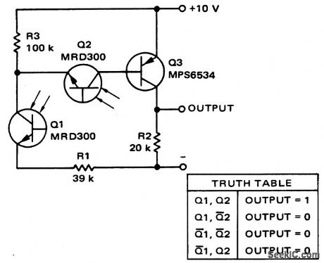
Photo-activated logic driver (courtesy Motorola Semiconductor Products Inc.). (View)
View full Circuit Diagram | Comments | Reading(646)
ELECTRONIC_SWITCH_FOR_RADAR_INDICA_TOR
Published:2009/7/17 5:15:00 Author:Jessie
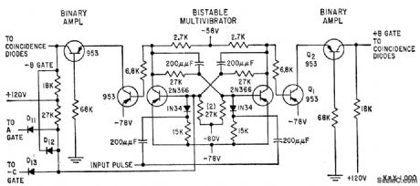
Used to produce aircraft identification markers on ppi. Coincidence of binary voltages supplies gating signals for switch.-J. B. Beach, Coincidence Diodes Gate Electronic Switch, Electronics, 32:8, p 66-68. (View)
View full Circuit Diagram | Comments | Reading(612)
Photo_activated_logic_driver_2
Published:2009/7/17 5:14:00 Author:Jessie
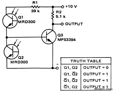
Photo-activated logic driver (courtesy Motorola Semiconductor Products Inc.). (View)
View full Circuit Diagram | Comments | Reading(664)
VIDEO_SWITCH
Published:2009/7/17 5:14:00 Author:Jessie
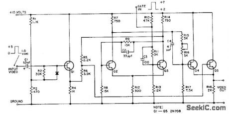
Used to either pass to blank out video signals going to ppi visual display. Blanking gate input pulse is applied to switch if video fails to identify itself as signal from associated radar set.-L. Turf, Video Switch for Radar, FEE, 11:2, p 24-25. (View)
View full Circuit Diagram | Comments | Reading(0)
Photo_activated_logic_driver_1
Published:2009/7/17 5:03:00 Author:Jessie
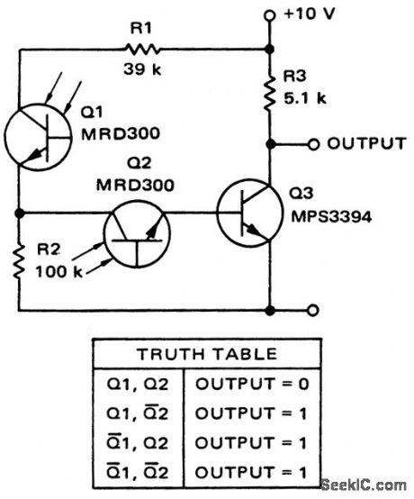
Photo-activated logic driver (courtesy Motorola Semiconductor Products Inc.). (View)
View full Circuit Diagram | Comments | Reading(691)
Photo_activated_logic_driver
Published:2009/7/17 5:01:00 Author:Jessie
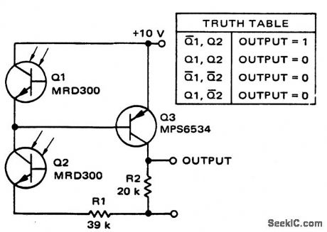
Photo-activated logic driver(courtesy Motorola semiconductor Products Inc.). (View)
View full Circuit Diagram | Comments | Reading(829)
AUDIO_VIDEO_SWITCHER
Published:2009/7/10 5:14:00 Author:May
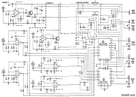
This circuit is a two-channel baseband video switcher. Buffer amps U1/Q1, U4/Q4, and associated components produce a buffered 75-Ω video signal, which is routed to switching network K1/K2/K3. Relay K1 selects either of these two video amplifiers and feeds J7. K2 also routup of either video amplifier to K3, which passes the selected video channel to J8 or connects J9 to J8.U2 andJ3 are audio amplifiers,which drive U7 and J8(CD4053 analog switches)to route audio from J1 and J2 to either J14/J15,or J10/J11.Also,audio from J12/J13 can be routed to these jacks.
(View)
View full Circuit Diagram | Comments | Reading(3489)
PUSHBUTTON_CONTROLLED_POWER_SWITCH
Published:2009/7/10 5:13:00 Author:May
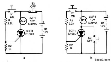
In both circuits, the SCR (and thereby the lamp) can be latched on by momentarily closing S1, thereby feeding gate drive to the SC via R1. In both circuits, the gate is tied to the cathode via R2 to improve circuit stability.Of course, after the SCR turns on, it can be tumed off again only by momentarily reducing anode current below the device's IH value. The SCR is tumed off by momentarily opening S2, by using S2 to short the anode and cathode terminals of the SCR momentarily. (View)
View full Circuit Diagram | Comments | Reading(1045)
UNIVERSAL_POWER_CONTROLLER
Published:2009/7/10 5:08:00 Author:May
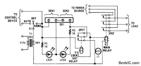
Relay K1 has a low-impedance coil and K2 has a high-impedance coil. When a sensor opens, current is routed through the coil of K1. K1 activates, opens its contacts, and prevents a sensor contact reclosure from affecting the circuit. When K1 contacts open, current to the main relay K2 is limited by the impedance of K1.K2 controls power to a load (air conditioner, furnace blower, etc.). (View)
View full Circuit Diagram | Comments | Reading(710)
N+1WIRES_CONNECT_N_HALL_EFFECT_SWITCHES
Published:2009/7/10 5:03:00 Author:May
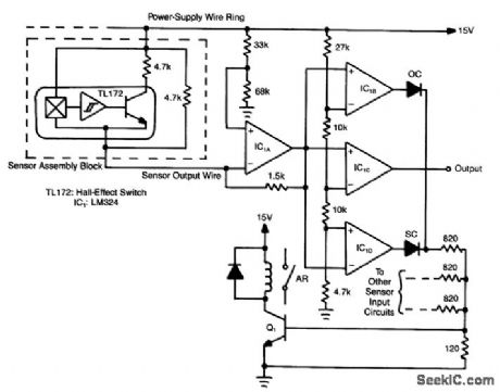
Hall-effect switches have several advantages over mechanically and optically coupled switches. Their major drawback is that they require three wires per device. This circuit, however, reduces this wire count to N + 1 wires for N devices.Amplifter IC1A is configured as a current-to-voltage converter. It senses the sensor assembly's output current. When the Hall-effect switch is actuated, the sensor's output current increases to twice its quiescent value. Amplifter IC1B, conftgured as a comparator, detects this increase. The comparator's output goes low when the Hall-effect switch turns on.The circuit also contains a fault-detection function. If any sensor output wire is open, its corresponding LED will turn on. If the power-supply line opens, several LEDs will tum on. A short circuit will also tum an LED on. Every time an LED tums on, Q1 turns on and the alarm relay is actuated.
(View)
View full Circuit Diagram | Comments | Reading(722)
dc_MILLIVOLTMETER
Published:2009/7/10 4:44:00 Author:May
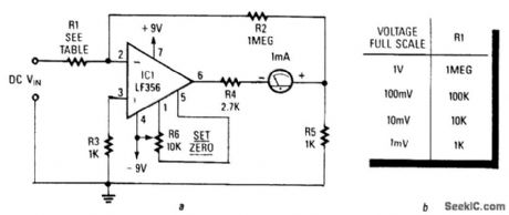
An LF356 op amp is used as a gain amplifter with the output taken across R5. When a full-scale current of 1 mA is flowing through the meter, exactly 1V appears across R5 (should be 1% tolerance or better). This is fed back to R2 to the summing junction of IC1 (a full-scale produces 1μA). This offsets the current through R1. R1 has a value of 1 MΩ/V which is used to zero the meter. R4 provides some overcur-rent protection for the meter. (View)
View full Circuit Diagram | Comments | Reading(2383)
LED_MILLIVOLTMETER
Published:2009/7/10 4:28:00 Author:May
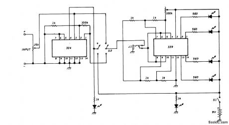
This circuit uses a dc amplifier (324) in a bar-graph circuit that uses an LM339 Quad comparator IC to sense dc levels.The LEDs will light every 100 mV.The 324 op amp is configured to provide a gain of 100×to increase this sensitivity to 1 mV.Two auxiliary LEDs indicate power on and ×100 gam setting. (View)
View full Circuit Diagram | Comments | Reading(2723)
CURRENT_LOOP_SCR_CONTROL
Published:2009/7/10 4:27:00 Author:May
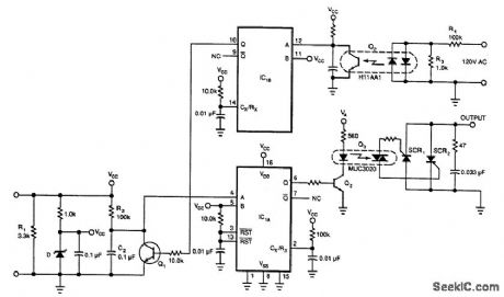
This circuit allows a 4-to 20-mA current loop to control an isolated SCR drive, IC1A and B are one-shots, Q2 detects zero crossings of the 120 Vac line, which trisaers one-shot IC1B. IC1A causes Q1 to discharge C2. When C2 recharges through Rz, it triggers IC1A, and the optoisolatoror and SCR1 /SCR2.Trig- gering of SCR1 and SCR2 is a function of input current, which can control motor speed, light intensity, etc. (View)
View full Circuit Diagram | Comments | Reading(1287)
POWER_MOSFET_SWITCH
Published:2009/7/10 4:15:00 Author:May

This solid-state switch senses and interrupts an overcurrent condition within 2μs. I1 allows the circuit to float. IC1 runs at 150 kHz and full-wave doubler D1/D2 provides 15 V to the gate of Q1. An overcurrent sensed across R1 triggers Q3, removes gate bias from Q1, and opens the circuit formed by the full-wave bridge and Q1. C1 and R3 allow the circuit to handle surges.
(View)
View full Circuit Diagram | Comments | Reading(1568)
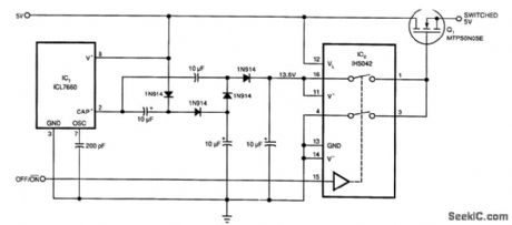
5_VSUPPLY_HIGH_SIDE_SWITCHER
Published:2009/7/10 4:07:00 Author:May
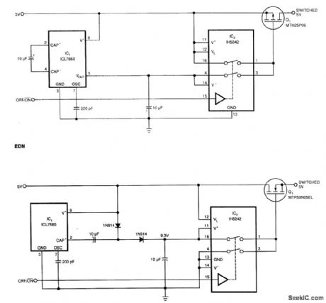
Requiring only 10 uA of quiescent current, the circuit of (Fig. 62-1(a)) produces only 0.1-Ω ON-resis-tance. IC1 is a charge pump voltage converter to produce a -5-V level, so analog switch IC2 can provide a 10-V swing to MOSFET Q1.
This circuit uses a voltage converter to enable the analog switch to apply a 4.3-V swing to logic level NMOS power transistor Q1. ON resistance is 0.03 Ω typical.
This circuit uses additional stages in the voltage-multiplying circuit to provide a higher gate voltage swing. This would enable the use of a convener for an NMOS switching transistor. (View)
View full Circuit Diagram | Comments | Reading(772)
FAST_DUMP_SWITCH_
Published:2009/7/10 3:46:00 Author:May
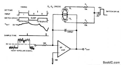


Requires only 350 ns to dump 6-V output to level of 3 mV. Transistors are connected so one of them is biased in forward mode independently of output polarity. Both transistors tum on during dump interval.Transistor operating in forward mode determines initial discharge rate until it saturates, after which inverted-mode transistorcontinuesto discharge capacitor. Offset voltage error is only -25 μV. Opamp is Analog Devices 120 or equivalent having unityqain bandwidth above 100 MHz and slew rate above 200 V/us.-F. Tarico, Fast Bipolar Dump Switch Has Low Offset, EDN Magazine,Nov5,1974.p 66. (View)
View full Circuit Diagram | Comments | Reading(778)
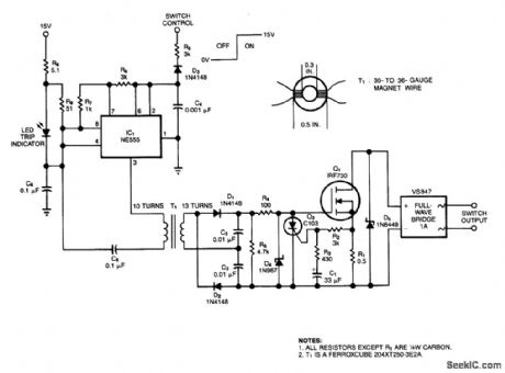
DETECTOR_AND_CONTROLLER
Published:2009/7/10 3:46:00 Author:May
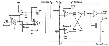
Many applications require analog signals to be sensed and digital signals to be controlled. A way to detect these points is by using a 555 timer in an unconventional configuration. This method will also add hysteresis to the circuit and guard against oscillation. The 555 supplies two comparators and a flip-flop eliminates the oscillation. Using this classic timer in the new configuration also reduces the component count.
The circuit shows the 555's trigger and threshold pins tied together. This enables the comparators to set and reset the flip-flop. Op amp U2 supplies both the trip-point setting and a way to adjust the hysteresis for ON and OFF points. One application where this circuit would be useful is in a Nicad battery-charge controller. (View)
View full Circuit Diagram | Comments | Reading(693)
MICROPHONE_CONTROLLED_VOICEACTIVATED_SWITCH
Published:2009/7/10 3:31:00 Author:May
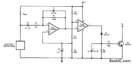
An electret microphone feeds a bandpass ftlter circuit (IC1A), then feeds a comparator, which in turn drives Q1. Q1 is a switch that conducts when audio from IC1B causes D1. C4. R6. and R7 to bias it oN. (View)
View full Circuit Diagram | Comments | Reading(837)
ONE_MOSPOWER_FET_ANALOG_SWITCH
Published:2009/7/10 3:26:00 Author:May
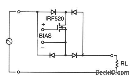
Using four diode in an array allows using only one MOSPOWER transistor for analog switching.The current flow is controlled by keeping the source-base connection of the MOSFET towards the load. Be sure to use diodes capable of handling the load current and a transistor whose breakdown voltage specification exceeds the peak analog voltage anticipated. Operationally, by increasing the gate-to-source bias voltage, the MOSFET turns on. For applications other than either full-on or full-off, care must be taken not to exceed the dissipation of the MOSPOWER transistor. A suitable heatsink cannot be overstressed in such applications. (View)
View full Circuit Diagram | Comments | Reading(914)
RF_POWER_SWITCH
Published:2009/7/10 3:20:00 Author:May
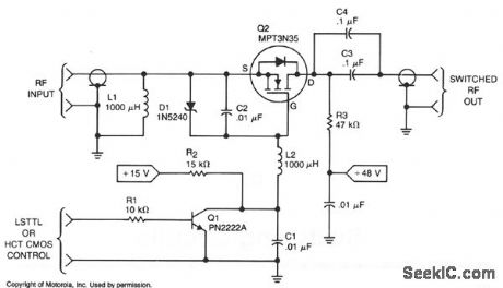
This rf power switch operates at 1.7 MHz with a 50-V Source and load.Its on loss is 0.2 dB and its off isolation is 30 dB.It provides 40-W PEP,45 VPEAK and 0.9 APEAK. The control input can come from CMOS ,TTL,LS,etc.,to turn on Q1,which turns on Q2,a TMOS MTP3N35. (View)
View full Circuit Diagram | Comments | Reading(937)
| Pages:113/312 At 20101102103104105106107108109110111112113114115116117118119120Under 20 |
Circuit Categories
power supply circuit
Amplifier Circuit
Basic Circuit
LED and Light Circuit
Sensor Circuit
Signal Processing
Electrical Equipment Circuit
Control Circuit
Remote Control Circuit
A/D-D/A Converter Circuit
Audio Circuit
Measuring and Test Circuit
Communication Circuit
Computer-Related Circuit
555 Circuit
Automotive Circuit
Repairing Circuit