
Control Circuit
Index 117
WIRELESS_REMOTE_TU_NING
Published:2009/7/20 1:49:00 Author:Jessie
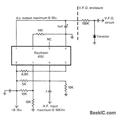
Frequency-to-voltage converter for transceiver responds to AF output of control receiver and feeds corresponding DC voltage to varactor tuning diode in VFO of transceiver, for remote wireless tuning. In most cases only a few volts of DC variation across varactor are sufficient, so variable audio oscillator at remote-control location need have range of only a few kilohertz.-J. Schultz, H.F. Operating-Remote Control Style, CQ, March 1978, p 22-23 and 90. (View)
View full Circuit Diagram | Comments | Reading(668)
3_μP_I_O_LINE_PROTECTORS
Published:2009/7/9 22:51:00 Author:May

In Fig. 20-3(a), a 5.1-V zener diode clamps positive-going transients, and a Schottky rectifier clamps negative-going transients. The Schottky rectifier has problems at both ends or the temperature scale. At 125℃ (2570F), its leakage current can reach 50 μA when the input line is at 5 V. This leakage is not a big deal unless the input resistor has a value of 100 kΩ or more. More troubling, at temperatures below -40℃ (-400F), the Schottky rectifier's forward voltage rises to about 0.47 V, which is perilously close to the -0.50 -V max spec that most HCMOS-type μPs inputs can tolerate.
The third circuit, Fig. 20-3(c), uses two regular silicon rectifiers. One rectifier is connected in series with the input line, thereby isolating the μPs inputs from negative-going voltage spikes. The other recti-fter is in series with a 5.1-V zener, which clamps positive-going transients. (View)
View full Circuit Diagram | Comments | Reading(878)
FOUR_QUADRANT_DIMMER
Published:2009/7/9 22:47:00 Author:May
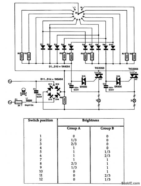
This very special mains-operated dimmer for domestic or industrial lights is not available in proprie-tary form: it enables brightness control of two groups of lights in one operation. The possible combinations of brightness are shown itt the table. It will be clear that it is not possible to obtain continuous brightness control in the two groups. Instead, the circuit affords the setting of four states of brightness in either group: full on, fully dimmed, 1/3 on, and 2/3 on.
Both sections of the circuit operate on the well-known principle of the triac being switched from the blocking state to the conducting state with the aid of an RC network and a diode. The RC network provides the necessary phase shift and determines when the triac is switched. The rotary switch selects the resis-tor in a given network, and thus the brightness of the relevant group of lights. No resistor means that the group is off; a short-circuit gives maximum brightness, and resistors of 10 k0 and 18 k0 produce interme-diate brightness. The diodes prevent the groups from affecting one another.
The 64-μH choke (L1) and the 150 nF capacitor across the bridge rectifier prevent the dimmer caus-ing interference in other equipment connected to the mains.
If the triacs are fitted on a heatsink that is rated at 12°K/W, up to 500 W per group can be controlled.It is, of course, essential that the enclosure in which the dimmer is fitted provides ample cooling. A fair number of slots or holes in it are, therefore, essential; these should not permit the circuit elements to be touched.
The switch should have a nonmetallic spindle: this is not only safer than a metallic one, but it also enables the easy removal of the end-notch so that the switch can be rotated continuously, instead of having to be returned to the first stop every time it is operated.
The mains on/off switch S2 should be fitted with a built-in ON indicator bulb, which shows at a glance whether the circuit is on, even though S1 might be in the OFF position. Finally, remember that this circuit carries mains voltage in many places: good workmanship and insulation are, therefore, of the utmost importance. (View)
View full Circuit Diagram | Comments | Reading(1109)
TACHOMETERLESS_MOTOR_SPEED_CONTROL
Published:2009/7/9 22:44:00 Author:May

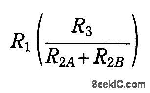


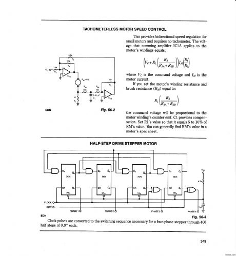


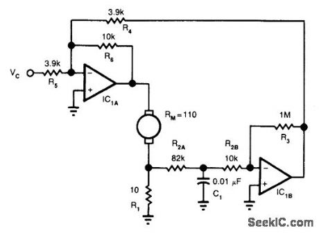

This provides bidirectional speed regulation for small motors and requires no tachometer. The volt-age that summing amplifier IC1A applies to the motor's windings equals:whereVCis the command voltage and IM is the motor current.If you set the motor's winding resistance and brush resistance(RM)equal to:the command voltage will be proportional to the motor winding's counter emf. C1 provides compen-sation. Set R1's value so that it equals 5 to 10% of RM's value. You can generally find RM's value in a motor's spec sheet. (View)
View full Circuit Diagram | Comments | Reading(614)
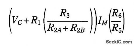
LIGHT_DIMMER_SPEED_CONTROL
Published:2009/7/9 22:39:00 Author:May
A phase-controlled triac (HT-32) circuit provides control of effective voltage at load. Do not omit L1 and C4 because they are for RFI suppression. The maximum load is about 500W. WARNING: 120 Vac is present on this circuit-provide adequate insulation and construction techniques. (View)
View full Circuit Diagram | Comments | Reading(699)
MINI_DRILL_CONTROL
Published:2009/7/9 22:36:00 Author:May


This circuit is intended as a revolution control for small dc motors as fitted, for instance, in small elec-tric drills (such as used for precision engineering and for drilling boards,among others). The behavior of these motors, which are normally permanent magnet types, is comparable to that of dependently pow-ered motors.In theory, the rpm of these motors depends solely on the applied voltage. The motor adjusts its rpm until the counter emf generated in its coils is equal to the applied voltage. There is, unfortunately, a drop across the internal resistance of the motor, which causes the rpm to drop in relation to the load. In other words, the larger the load, the larger the drop across the internal resistance and the lower the rpm.This circuit provides a kind of compensation for the internal resistance of the motor: when the urrent drawn by the motor rises, the supply voltage is increased automatically to counter the fall in rpm.The circuit is based on an enhanced voltage regulator that consists of IC1 and T1, which provides a easonably large output current (even small drills draw 2-to-5 A). The onset supply voltage, and thus the ram, is set by P2. Because of emitter resistance R1, the currents through IC1 and T1 will be related to one another in the ratio that is determined by R1 and R2. Owing to this arrangement, the internal short-circuit protection of IC1 will also, indirectly, provide some protection to T1.As soon as the current drawn exceeds a certain value, T2 will be switched on. This results in a base current for T3 so that R5 is in parallel (more or less) with R6. This arrangement automatically raises the output voltage to counter a threatened drop in rpm. The moment at which this action occurs is set by P1, so this circuit can be adapted pretty precisely to the motor used.If only very small motors are likely to be used, the power supply (transformer and bridge rectifier) can be rated more conservatively. As a guide, the current in the transformer secondary should be about 1.5 times the maximum dc output current. (View)
View full Circuit Diagram | Comments | Reading(3242)
FREQUENCY_SHIFT_KEYER
Published:2009/7/9 22:33:00 Author:May

Apply a signal to each differential amplifier input pair.When the gate voltage is changed from oneextreme to the other, the output can be switched alternately between the two input signals.When the gatelevel is high (1.5V), a signal applied between pms 5 and 6(channel A)will be passed and a signal appliedbetween pins 3 and 4(channel B)will be suppressed.In this manner,a binary-to-frequency conversion is obtained that is directly related to the binary sequence,which is driving the gate mput (pin 2). (View)
View full Circuit Diagram | Comments | Reading(683)
TRANSMITTER_NEGATIVE_KEY_LINE_KEYER
Published:2009/7/9 22:29:00 Author:May
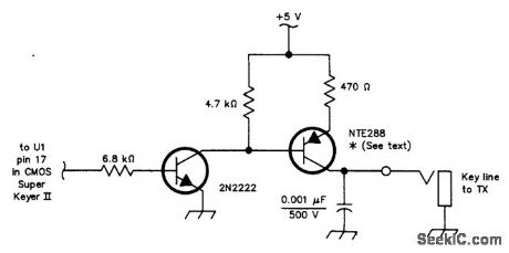
Using an NTE288 (or ECG288, GE223, or SK3434), this circuit can key a negative line up to-300V maximum. Do not use this circuit to key a vacuum-tube amplifier that draws grid current because the keying transistor might be damaged under these conditions. (View)
View full Circuit Diagram | Comments | Reading(772)
CW_KEYER
Published:2009/7/9 22:27:00 Author:May

This electronic keyer uses four ICs (five, if the optional sidetone oscillator is desired) and operates from dc sources of 9 to 15V. A 2N2222 is used as a keying transistor. If isolators or more power handling ability is desired, a 6-V relay can be keyed with the 2N2222 and the relay in turn can be used to key the transmitter. (View)
View full Circuit Diagram | Comments | Reading(1531)
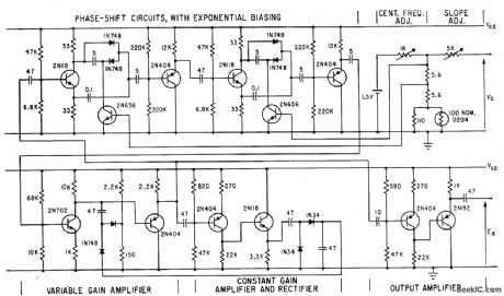
SELF_SYNCHRONIZED_PHASE_SHIFTER
Published:2009/7/20 3:32:00 Author:Jessie
Consists of power supply, inverter, phase-shifting Selsyn, 100-cps filter, and output amplifier, used to vary phase of 100-cps frequency standard output by synchronization with WWV for studies of low-frequency propagation over long distances.-M. M. Newman etal, Sea-Going Lightning Generator, Electronics, 33:30, p 53-55. (View)
View full Circuit Diagram | Comments | Reading(1201)
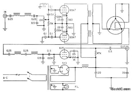
ANTENNA_PHASING_CONTROL
Published:2009/7/20 3:21:00 Author:Jessie
Used with two antennas on different parts of an aircraft to insert artificial delay in series with one antenna so signal addition will occur. Contains staircase generator that charges C1 in steps until receiver threshold cuts off V2. Charge on C1 biases V5 to change magnetization of reactor and thereby lock phaser automatically at optimum degree of delay.-I. Dlugatch, Optimizing Antenna Switches and Phasers, Electronics, 32:33, p 55-57. (View)
View full Circuit Diagram | Comments | Reading(744)
CONTINUOUS_PHASE_CONTROL
Published:2009/7/20 3:16:00 Author:Jessie
Potentiometer changes phase relationship between synchronizing voltage V1 and output voltage V2, without affecting amplitude of output from free-running mvbr.-S. Tesic, Multivibrator Provides Continuous Phase Control, Electronics, 39:15, p 102-103. (View)
View full Circuit Diagram | Comments | Reading(763)
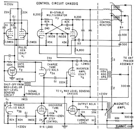
AUDIO_CONTROL_FOR_ANTENNA_PHASER
Published:2009/7/20 3:15:00 Author:Jessie
Rectified audio in multiple-antenna aircraft receiver alternately charges C2 and C3 at grids of V2. Bistable mvbr V3 performs switching in synchronism with pulse generator so each switch position corresponds to change in antenna phasing. When peak of signal is passed and phase is reversed, V4 pulls in K1 and sends control signal to control unit. K2 opens when difference in potentials of C2 and C3 becomes excessive, forcing system to resume cycling until output is again maximized.-I. Dlugatch, Optimizing Antenna Switches and Phasers, Electronics, 32:33, p 55-57. (View)
View full Circuit Diagram | Comments | Reading(761)
CMOS_SHORT_PULSE_GENERATOR
Published:2009/7/9 21:48:00 Author:May
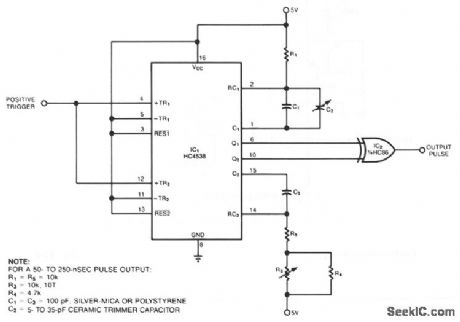
Comprising two low-power, CMOS chips, the pulse generator produces a precise pulse width in the 50 to 500 ns range. IC1 is a dual monostable multivibrator (one shot) in which each positive trigger pulse initiates simultaneous positive output pulses at pins 6 and 10. In response, XOR gate IC2 produces a positive pulse whose duration is equal to the difference between the two input-pulse durations. Section 1 of the one shot generates an approximate 1-μs reference pulse-shorter pulses are more susceptible to manu-facturing variations caused by parasitic layout capacitance. Variable capacitor C2 lets you adjust this pulse width. Section 2 of the one shot generates a variable-length pulse; you adjust its width by using potentiometer R3. Resistors R4 and R5 set the output pulse's maximum and minimum width, respectively. Because the XOR gate's rise and fall times are about 20 ns for reasonable values of load capacitance, you should calibrate the circuit using C2 for a minimum output-width of 50 ns. (View)
View full Circuit Diagram | Comments | Reading(1767)
BURGLAR_ALARM_WITH_NC_AND_NO_SWITCHES
Published:2009/7/9 21:47:00 Author:May
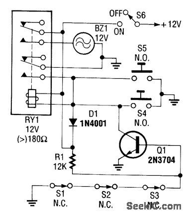
This circuit uses both NC and N0 sensors. Series NC sensors allow Q1 to activate RY1. NO sensors directly activate RY1. (View)
View full Circuit Diagram | Comments | Reading(765)
SIMPLE_BURGLAR_ALARM_WITH_NC_SWITCHES
Published:2009/7/9 21:46:00 Author:May

This relay draws 1 mA of idling current. Q1 detects open switch and energizes RY1. (View)
View full Circuit Diagram | Comments | Reading(718)
SIMPLE_BURGLAR_ALARM_1
Published:2009/7/9 21:41:00 Author:May
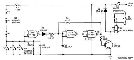
Using one IC and a driver transistor, this simple alarm uses either NO or NC sensors,When a sensoroperates,the input to U1A goes low,causmg U1A to go high,U1B low,and U1C high.This biases Q1 ONand activates relay K1.On/offis vla keyswitch S1. (View)
View full Circuit Diagram | Comments | Reading(798)
SIMPLE_BURGLAR_ALARM
Published:2009/7/9 21:39:00 Author:May
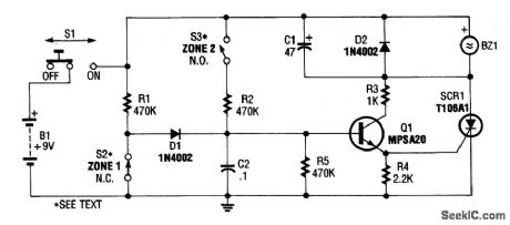
A simple circuit using either NO or NC sensors uses an RC delay circuit (R2/C2 or R1/C2) to drive emitter-follower Q1, switching SCR1 and buzzer (or bell) BZ1. S1 is used for activation and reset. (View)
View full Circuit Diagram | Comments | Reading(905)
SCR_PROXIMITY_ALARM
Published:2009/7/9 21:38:00 Author:May
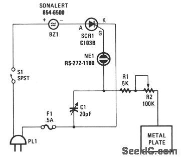
View full Circuit Diagram | Comments | Reading(766)
VOLTAGE_CONTROLLED_PHASE_SHIFT_OSCILLATOR
Published:2009/7/20 4:27:00 Author:Jessie
Small-signal a-c resistance of junction diode, related to reciprocal of junction current over two-decade range, is used in two-section R-C phase-shift network acting with amplifier and agc to give constant-amplitude voltage-controlled oscillator with frequency range of over two decades.-R. A. Greiner and S. K. Morgan, Voltage Controlled Wide-Range Oscillator, Electronics, 34:51, p 31-35. (View)
View full Circuit Diagram | Comments | Reading(1575)
| Pages:117/312 At 20101102103104105106107108109110111112113114115116117118119120Under 20 |
Circuit Categories
power supply circuit
Amplifier Circuit
Basic Circuit
LED and Light Circuit
Sensor Circuit
Signal Processing
Electrical Equipment Circuit
Control Circuit
Remote Control Circuit
A/D-D/A Converter Circuit
Audio Circuit
Measuring and Test Circuit
Communication Circuit
Computer-Related Circuit
555 Circuit
Automotive Circuit
Repairing Circuit