
Control Circuit
Index 109
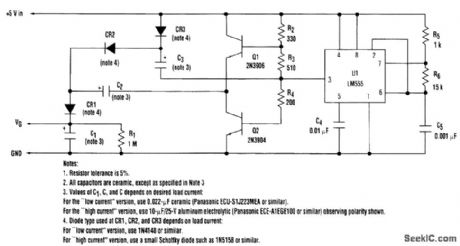
SNAP_ACTION_A_F_POWER_LEVEL_SWITCH
Published:2009/7/12 22:21:00 Author:May
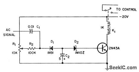
When integated voltage reaches point where zener diode breaks from nonconduction to conduction, transistor goes from cutoff to saturation suddenly, to provide fast relay operation.-Snap Action Level Switch, Electronic Circuit Design Handbook, Mactier Pub.Corp. N.Y. p30. (View)
View full Circuit Diagram | Comments | Reading(779)
INTRUDER_ALARM
Published:2009/7/12 22:21:00 Author:May
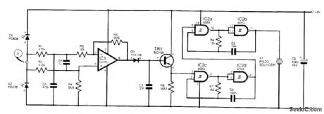
The circuit triggers a pulsed-tone alarm when anyone passes by, and several of these units can be scattered around the premises to give burglars the impression that they are being monitored! It is guaranteed to drive any burglar bananas. Two photodiodes, D1 and D2, are used as shown to ensure sensitivity over a very wide range of lightning conditions, though the circuit will be less effective in diffuse light. IC1 is connected as a differential amplifier. As thevoltage at pointA swings high, the response at pin 2 of IC1 is slowed by capacitor C1, and the voltage swings high at the output (pin 6). Capacitor C3 charges up and transistor TR1 level-shifts the signal to enable the oscillator section formed from IC2, a quad NAND Schmitt. The piezo disk X1 will pulse accordingly. C3 determines the duration of the pulsed tone and resistor R8 determines the pitch. Photodiodes D1 and D2 should be mounted a small distance apart for best effect. The circuit draws a mere 0.5 mA.
(View)
View full Circuit Diagram | Comments | Reading(0)
MAGNETRON_BEAM_SWITCHING
Published:2009/7/16 22:49:00 Author:Jessie
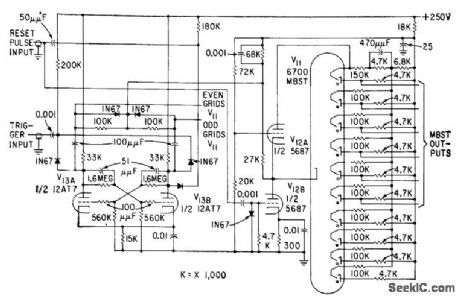
First trigger pulse switches beam to first position, and each succeeding trigger advances beam one position, until reset pulse zeroes V11 for repetition of switching sequence. Succeeding switching-circuit output pulses are thus time-coincident with succeeding amplitude portions of input signal, for pulse amplitude measurement.-J. F. Lyons, Jr., Analyzing Multipath Delay in Communications Studies, Electronics, 32:36, p 52-55. (View)
View full Circuit Diagram | Comments | Reading(728)
FEEDBACK_CONTROL_FOR_MAX253
Published:2009/7/16 22:42:00 Author:Jessie
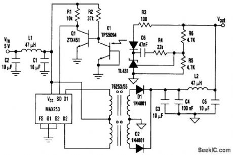
The MAX253 and associated 76253 transformers were designed to allow easy implementation of simple dc-to-dc converter circuits. The main problem with the basic circuit is that there is no feed-back, resulting in no control over the output voltage at light loads. When transformer isolators designed for 1-W power levels are used, output voltages can be observed rising above 5.5 V at less than 20-percent load. The circuit provides feedback control from the output via an optoisolator and voltage-reference device in a single pack (TPS5094). This results in an output voltage that is static at light loads. The circuit uses the internal TL431 reference devices of the TPS5904 to set a value at which the optoisolator is switched (Vref = 2.51 V). Using two 4.7-kΩ resistors (R5 and R6) gives an ideal output voltage of 5 V; with only 500μA of drain current, the measured value was 4.95 V. The output of the optoisolator then controls the shutdown pin (SD) on the MAX253, via the ZTX451 buffer transistor, and switches the device off when the output voltage exceeds the predefined value. Therefore, the circuit works in a burst mode at light loads, with the switching being turned on and off as necessary. As the load increases, the device eventually reaches the stage where switching is occurring all the time. (View)
View full Circuit Diagram | Comments | Reading(907)
Pull-push switch circuit diagram
Published:2011/7/20 5:29:00 Author:nelly | Keyword: Pull-push switch
As shown in the figure, it is the pull-push switch circuit which is composed of P channel and channel power MOSFET transistor, it does not require bootstrap circuit.
(View)
View full Circuit Diagram | Comments | Reading(843)
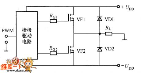
Advanced drive circuit diagram
Published:2011/7/20 5:34:00 Author:nelly | Keyword: drive

As shown in the figure, it is the advanced drive circuit which is composed of P channel power MOSFET, one terminal of the load is ground connection, it does not require bootstrap circuit, so it is mainly used in lower voltage switch circuit.
(View)
View full Circuit Diagram | Comments | Reading(649)
GENERIC_TAIAC_SWITCH_INTERFACE_FOR_RESISTIVEL_LOAD
Published:2009/7/17 1:29:00 Author:Jessie
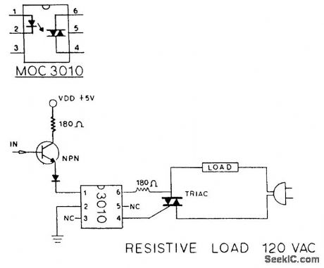
A TTL level input turns on the MOC3010 optocoupler and triggers the triac,applytng 120 Vac tothe load. (View)
View full Circuit Diagram | Comments | Reading(3395)
CUT_PHONE_LINE_ALARM
Published:2009/7/12 22:16:00 Author:May
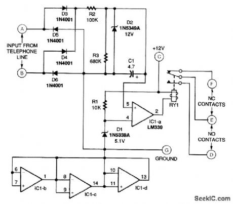
The figure shows the schematic diagram of the phone line monitor. Note that 12-Vdc power is connected to the unit via solder pads C (positive) and G(ground) on the PC board. This power should be supplied from your home security system, since it will have battery backup, and this will be as reliable as your base security system. The input from the telephone line is fed to pads A and B. Polarity is not important to the monitor because the input is rectified by the full-wave bridge rectifer formed by diodes D3 to D6. Connecting the phone line to the phone line monitor in no way diminishes phone senrtce', and its presence on the line will be unnoticed by you and those who call you. The rectified or polarized voltage from the bridge rectifier is fed to a long-time-constant filter formed by R2 and C1. This filter includes a zener diode (D2) that limits the voltage maximum charge on C1 to 12 V during normal operation. Resistor R3 provides a high-resistance shorting path to drain the charge from C1 when there is no input voltage. This resistor sets the time delay for activating the alarm. The trigger voltage for comparator IC1-a is generated by R1 and D1. Diode Dl is a 5.1-V zener whose output is fed to the inverting input (pin 4) of IC1-a. With the inverting input at 5.1 V, any voltage above 5.1 Y on the noninverting input (pin 5) will cause the output of the comparator to go high. Since the output of IC1 is tied to the relay coil of RY1 and the other end of the relay is tied to +12 Vdc, the relay coil is not energized. When the voltage from the input filter drops below 5.1 V, the out-put of IC1-a goes low and energizes the relay. The contacts of RY1 (either the normally open set or the normally closed set) could also be used to trigger the home's security system.
(View)
View full Circuit Diagram | Comments | Reading(1348)
SCSI_SWITCH
Published:2009/7/12 21:51:00 Author:May
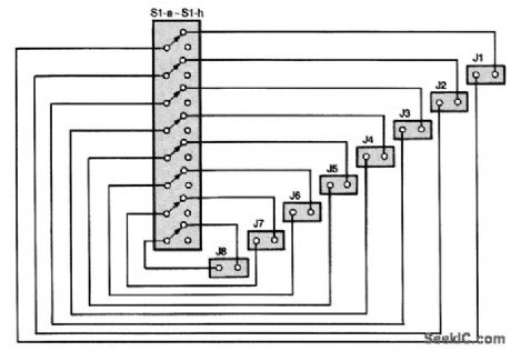
The SCSI switch consists of an eight-position DIP switch, about 24 inches of ribbon cable, and eight female header blocks. A schematic of the switch is shown. The header blocks plug onto the ID pins of the SCSI hard disks. Through the DIP switch, those IDs can be reassigned at will. In any given configuration, whichever physical drive has the lowest SCSI ID becomes the boot drive. The others are allocated in order by SCSI ID. (View)
View full Circuit Diagram | Comments | Reading(853)
AC_CONTROL_WITH_TRIAC
Published:2009/7/12 21:34:00 Author:May
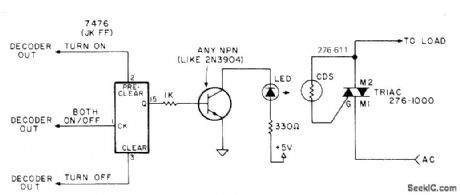
Decoder outputs of microprocessor feed 7476 JK fliρ-floρ thatdrives optocoupler which triggers triac for ON/OFF control of lamp or other AC load. LED andcadmium sulfide photocell are mounted in light shield. When light fron LED is on photocell, cell resistance drops and allows control voltage of correct direction and amplitude to trigger gate of triac, turning it on. When light disappears,triac remains on until voltage falls near zero in AC cycle.-R. Wright, Utilize ASCLL Control Codes!, Kilobaud, Oct, 1977, p 80-83. (View)
View full Circuit Diagram | Comments | Reading(1578)
COMPUTER_SERIAL_PORT_RELAY_CONTROLLER
Published:2009/7/12 21:03:00 Author:May
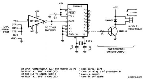
Decoding RS-232 signais is a job for a microcontroller (single-chip computer). Fortunately, you don't have to program the microcontroller yourself; you can get a PIC 16C54A microcontroller already programmed for exactly this job from Stone Mountain Instruments. Shown is the circuit and the BASIC program to demonstrate how it works. Each SMI101B has eight logic-level outputs.Further, you can connect up to seven SMI101Bs to a single serial port. The three N pins give each SMI101B a distinctive identifying number, from 0 to 6. If all three are grounded, the identifier is 0; if N1 is connected to +5 V, the identifier is 1, etc. At power-up, all the data outputs are off (logic 0). To turn an output on, send a command of the form xNy, where x is the identifier of the SMI101B and y indicates which data output you want to switch, To turn the outputs back off, use an F in place of an N (e.g., OF3). All communication is done with 8 data bits and no parity bits. The baud rate is 9600 baud with a 4-MHz crystal, or 1200 baud with a 500-kHz ceramic resonator. As shown in the diagram, each relay requires a transistor to drive it, along with a resistor and a protective diode. To cut down the total number of components, you can use a relay driver chip, such as the Allegro UDN2987, which contains everything necessary to drive eight small relays from logic-level signals. (View)
View full Circuit Diagram | Comments | Reading(2267)
DIGITAL_VOLUME_CONTROL
Published:2009/7/12 20:37:00 Author:May
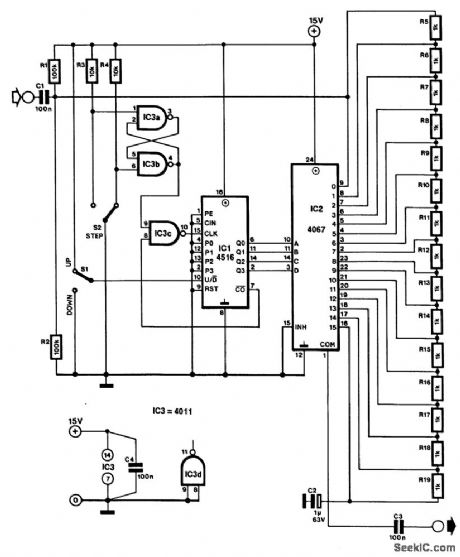
The heart of the digitally operated volume control is IC2, a 4067 16-channel analog multiplexer. Depending on the logic state on pins A, B, C, and D of the multiplexer, one of its 16 inputs or outputs is connected to pin 1, which is the wiper of the control. Because a 1-kΩ resistor has been connected between each input and output, the multiplexer can be considered a linear potentiometer with 16 fixed steps. Its overall resistance is 15 kΩ. It is, of course, possible to use a different value for each of the resistors to obtain a different characteristic. The setting of the potentiometer is controlled by counter IC1. Dependent on the position of switch S1, the counter moves one step up or down when switch S1 is changed over. Circuits IC3A and IC3B debounce S2.A jump from 0000 to 1111 or the other way around is not possible, because further count pulses are suppressed with the aid of the CO line. This line is logic low when both the counter state and signal U/D are 0.When U/D is high and the counter state is 15, COagain becomes logic low. It is then necessary to reverse the logic state at U/D, and thus the direction of counting. The volume control draws a current of around 1 mA. (View)
View full Circuit Diagram | Comments | Reading(5813)
TRANSIENT_SWITCH_SIGNAL_SUPPRESSOR
Published:2009/7/17 2:30:00 Author:Jessie
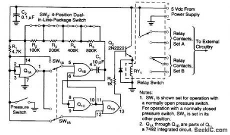
The figure shows a circuit that delays the transmission of a switch-opening or switch-closing signal until after a preset suppression time. The circuit is used to prevent the transmission of an undesired momentary switch signal. For example, a pressure switch that is meant to be held steadily on or off by a given static pressure in a piping system can also be actuated momentarily by a transient overpressure (sometimes called water hammef') or underpressure caused by the sudden closure or opening of a valve. The basic mode of operation is simple. The beginning of the switch signal initiates a timing sequence. If the switch signal persists after the preset suppression time, then this circuit transmits the switch signal to the external circuitry. If the switch signal is no longer present after the suppression time, then the switch signal is deemed to be transient, and this circuit does not pass the signal on to the external circuitry. From the perspective of the external circuitry, it is as though there were no transient switch signal. The suppression time is preset at a value large enough to allow for the damping of the underlying pressure wave or other mechanical transient. (View)
View full Circuit Diagram | Comments | Reading(857)
CHARGE_PUMP_GENERATING_GATE_DRIVE
Published:2009/7/17 2:13:00 Author:Jessie
A charge pump built as a voltage tripler can provide just the right amount of voltage needed for gate drive in a 5-V system. (View)
View full Circuit Diagram | Comments | Reading(868)
MIXER_FOR_DISTORTION_MONITOR
Published:2009/7/17 2:09:00 Author:Jessie
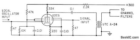
Combines local oscillator signal with two input-frequency tones without introducing distortion, by using primarily grid-swamping techniques.-G. H. Smith, Distortion Monitor Checks Linear Amplifier Characteristics, Electronics, 34:27, p 57-59. (View)
View full Circuit Diagram | Comments | Reading(697)
3_50WPM_KEYER
Published:2009/7/11 5:12:00 Author:May
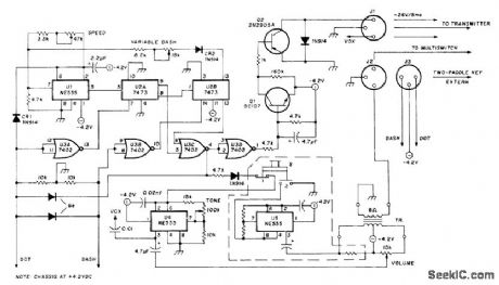
Uses NE555V 1 as switchable dot generator providing accurate 1 : 1 ratio.SN7473 U2 forms variable dash circuit. NE555V sidetone generator U4 has tone range of about three octaves and easily drives 3-W 4-ohm loudspeaker through small transistor-radio transformer TR. NE555V US acts with U4 to provide two-tone oscillator for SSB tuning. Output section Q1-Q2 easily handles keying bias of -26V at 5 mA.-H. Seeger, Micro-TO Keyer Mods,Ham Radio,July 1976,p 68-59. (View)
View full Circuit Diagram | Comments | Reading(1397)
SIMPLE_KEYER
Published:2009/7/11 4:56:00 Author:May
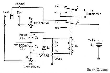
Based on rapid charging of capacitors and controlled discharge through relay coil. When C, has discharged to relay release voltage, relay drops out and cycle starts over again as long as dot side of paddle is pressed. Dashes are similarly formed by C1. R4 adjusts speed from 10 to 40 WPM. K1 is DPDT plate-current relay having 1K to 10K resistance.-J. J. Russo, An Inexpensive Electronic Keyer, CQ, Aug. 1971, p 58. (View)
View full Circuit Diagram | Comments | Reading(997)
TWO_STAGE_SWITCH
Published:2009/7/11 4:43:00 Author:May
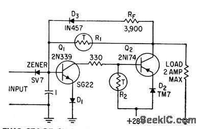
D-c output from carrier amplifer triggers switch consisting of two-stage complementary-coupled nonlinear am pliler, with zener diode in series with input to minimize drift, when difference between two d-c voltages exceeds preset threshold voltages of as little as 100 microvolts for only 300 microsec. Can handle 2 amp. R1 is 100,000 ohms and R2 is 100 ohms.-J. W. Hig-ginbotham and H. H. Douglass, Voltage Comparcttor with High-Speed Switches, Electronics, 32:5, p56--58. (View)
View full Circuit Diagram | Comments | Reading(861)
AUTOPILOT_COMPARATOR_ALARM
Published:2009/7/11 4:39:00 Author:May

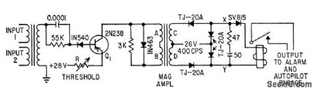
Actives alarm or disengages autopilot when signals from dual accelerometers differ apperciably.indicating malfunction.-C. W. McWilliams, Designing Safety Into Automotic Pilot Sys-tems, Electronics, 31:45, p69-71. (View)
View full Circuit Diagram | Comments | Reading(750)
CMOS_KEYER_3
Published:2009/7/11 4:30:00 Author:May

Uses two CD4001AE quad two-input N0R gates. Q1A-Q1B form time-base MVBR, and Q1C-Q1D form dash flip-flop. Three of remaining gates synthesize three-input NOB gate for dash control. Q2D controls time-base MVBR and provides keyer output. Speed is adjustable from below 10 to over 70 WPM with R3.-C. J. Bader, Improved CW Transceiver for 40 and 80 Ham Radio, July 1977, p 18-22. (View)
View full Circuit Diagram | Comments | Reading(875)
| Pages:109/312 At 20101102103104105106107108109110111112113114115116117118119120Under 20 |
Circuit Categories
power supply circuit
Amplifier Circuit
Basic Circuit
LED and Light Circuit
Sensor Circuit
Signal Processing
Electrical Equipment Circuit
Control Circuit
Remote Control Circuit
A/D-D/A Converter Circuit
Audio Circuit
Measuring and Test Circuit
Communication Circuit
Computer-Related Circuit
555 Circuit
Automotive Circuit
Repairing Circuit