
Control Circuit
Index 87
A number explicit expression timer circuit diagram
Published:2011/8/11 2:24:00 Author:Rebekka | Keyword: expression timer
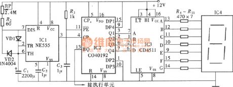
Digital display type timer has a clear display. It will show the digital pulse signal by digital display tube when the signal is coded by the number implement. This circuit introduces a digital display type timer. It's display unit is decided by the time-base signal. It can be a second and also can be the points or hour . But the digital display type timer for hour is too big. (View)
View full Circuit Diagram | Comments | Reading(1373)
High-precision adjustable digital timer circuit diagram
Published:2011/8/11 2:42:00 Author:Rebekka | Keyword: High-precision, adjustable digital timer
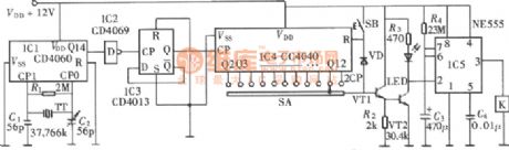

The high precision quartz crystal oscillator is composed of the CD4060 and the 32768 Hz ac quartz crystal. It passes the internal multi-stage and separates frequency output a precise second source. It can form a high precision adjustable digital timer by peripherals multi-stage separate frequency band. It can provide accurate time signal for some instruments, and it can also be used for the precise timing control of equipment. Its componentsare shown in figure. (View)
View full Circuit Diagram | Comments | Reading(2105)
High-precision time delay timing controller circuit diagram
Published:2011/8/11 2:40:00 Author:Rebekka | Keyword: High-precision , time delay, timing controller
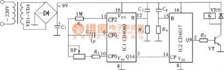
The low frequency RC roscillato oscillator is composed of CD4060 oscillator. It can output a long time base signal after passing the internal frequency division. When the long-time time base signal is divided by multi-level frequency again, a longer time delay time can be gotten, thenit form a high-precision time delay timing controller . The constitution circuit is shown as above. (View)
View full Circuit Diagram | Comments | Reading(1117)
Using temperature and frequency converter high-precision temperature control circuit diagram
Published:2011/8/9 2:28:00 Author:Rebekka | Keyword: high-precision temperature control
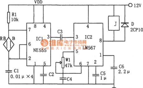
Because the RB changes with temperature, the fc also changes with temperature. Audio decoder phase lock loop uses a single audio decoder integrated circuit IC2 (LM567), the center frequency is xsl-fo = 1/1.1 Rw1C4. The adjustment of W1can setxsl-fotemperature frequency. When the IC1 oscillation frequency is the same with the center of the IC2, fc frequency xsl-fo is consistent. The LM567 outputs low level (8) foot) and makes relay J suck close. It will open the load. (View)
View full Circuit Diagram | Comments | Reading(1979)
Single-phase thyristor zero trigger electric stove temperature control circuit diagram
Published:2011/8/11 2:09:00 Author:Rebekka | Keyword: Single-phase thyristor, electric stove , zero trigger ,
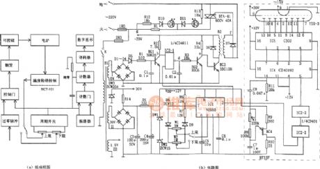
The figure shows the single-phase thyristor zero trigger electric furnace temperature control circuit. This temperature device is composed of the signal detection temperature control circuit, the zero detection circuit, cycle switch, trigger control and digital display etc. Itis used withXCT-101 temperature control meter together. It can monitor the 6 ~ 8 kW single-phase thyristor zero trigger electric furnace temperature. The temperature and thermal insulation are ajustable in 1% ~ 99%. The winding I1 of transformer B1, D1 ~ D4, D6, C1, BG1 and other components form the zero pulse detection circuit, IC2-l (1 / 4 CD4011) is the controlling door, and in the effect of the pulse output by cycle switch (IC1), it outputs a group of zero-crossing detection pulse, which is inverting amplified by BG2 and output by isolated transformer BG3. (View)
View full Circuit Diagram | Comments | Reading(3195)
Simple constant temperature controllor circuit composed of 555
Published:2011/8/9 2:17:00 Author:Rebekka | Keyword: Simple , constant temperature controllor
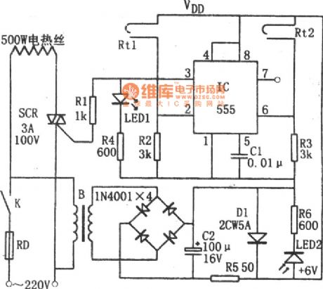
Rt1 contacts the contact because of the heated expansion, but IC 6 feet is disconnected since the Rt2 is still at the low level, thus the trigger circuit skins. The temperature continue to rise to the upper limit value, Rt2 is conducted, the corresponding 6 feet potential is inhigh level (6 V), it is larger than 6 x two-thirds = 4 V trigger level. The IC resets, the (3) foot outputs low level, SCR stops and the electric heating wires power supply is disconnected. It stops heating. When the temperature drops, Rt2 will be disconnected. For 555 circuit is self-preservation and it still outputs low level feet by (3). When the temperature drops to the limit value, Rt1 is disconnected. (View)
View full Circuit Diagram | Comments | Reading(724)
Developer temperature control circuit diagram
Published:2011/8/9 2:13:00 Author:Rebekka | Keyword: Developer temperature control
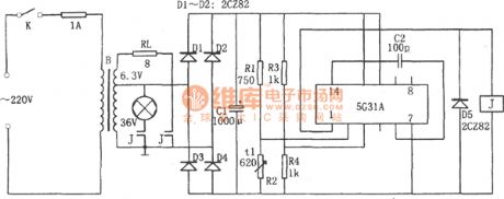
The figure shows the developer temperature control circuit. When the power supply is open, the temperature is low, the value of the R1 is high, so that the 5G31 outputs high level because the input potential of the positive end is higer than the input potential of the negative end.The relay J suck closes, RL starts to heat because the power supply is open and makes the temperature high. When the temperature rise to the control temperature, the bridge turns to balance. The 5G31 outputs low level because the potential of negative input terminal is higher than the positive input terminal . The relay J is disconnected, RL stops to heat because the power supply is closed. (View)
View full Circuit Diagram | Comments | Reading(645)
Multichannel pressure gauge inspection circuit diagram
Published:2011/8/15 2:35:00 Author:Rebekka | Keyword: Multichannel pressure , gauge inspection
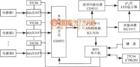
It uses more pieces of MAX1457 to match the monolithic A/D converter and single chip microcomputer to form the multi-channel pressure inspection instrument and the circuit diagram is shown as the chart. In the figure, it uses a piece of 8-1 analog switch CD4051 to receive 8-road sensor signals. The calibration coefficient of the each sensor is stored in 93C66. The output of the CD4051 connects with the ICL7135 4 1/2 bit monolithic A/D converter, then it uses the decoding driver (CD4511) and bit driver (MC1413) to drive 4 1/2 bit LED display. The 8051 single chip microcomputer decides one road sensor signal having completed A/d conversion by the DQS and BUSY signal output by ICL7135. (View)
View full Circuit Diagram | Comments | Reading(797)
Distance isolation temperature analog circuit diagram
Published:2011/8/16 2:52:00 Author:Rebekka | Keyword: Distance isolation , temperature analog
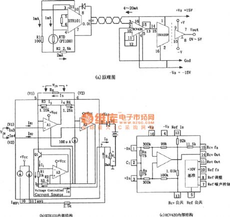

The figure shows the temperature analog circuit over long distances. In the practical application of the power system, the temperature of the equipment must be sent to the distance monitoring center, and it matchs with the measurement circuit, whichis isolated from the high voltage.In thecircuit, RTD is the platinum resistance temperature sensor, when the temperature rises, RTD resistance will be increased. The XTR101 has a high precision and WenPiao advantages, it can turn the temperature conversion into current signal, and it is easy to be transmitted over a long distance, because voltage signal in long-distance transmission loss error is large and vulnerable to electromagnetic interference.
(View)
View full Circuit Diagram | Comments | Reading(993)
1 ~ 5 V / 4 ~ 20 mA isolation converter circuit composed of the 3656 isolated amplifier
Published:2011/8/16 2:31:00 Author:Rebekka | Keyword: isolated amplifier , isolation converter
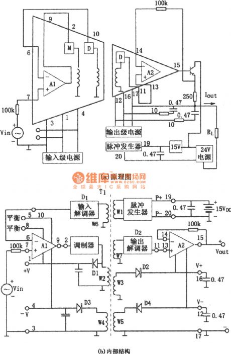
In the industrial real-time control system, in order to realize the long distance transmission signal, itoften needs to standard voltage signal 1 ~ 5 V switching for standard 4 to 20 mA current signal, because transmission current signal transmission loss is small, the low electromagnetic interference is low, it is also easy to identify, power lost or failure of open. Here 4 mA means zero level, 20 mA means the maximum signal. The figure shows the 1 ~ 5 V / 4 ~ 20 mA isolation converter composed of the 3656 isolated amplifier. Figure (b)shows 3656 internal structure.
(View)
View full Circuit Diagram | Comments | Reading(893)
The resistance strain guage application circuit diagram of ADT70ADT70 platinum RTD signal conditioner
Published:2011/8/16 2:23:00 Author:Rebekka | Keyword: resistance strain guage , application circuit , platinum RTD signal conditioner
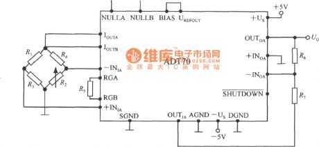
The application circuit of the ADT70 resistance strain instrument is shown in figure. The measurement bridge is composed of the temperature compensation chipR1, measurement strain gaugeR2, wire wound resistors R3, R4, its value is1 k Ω. The bridge road working currrent is provided by IOUTA and IOUTB. Each bridge arm passing current is 1 mA. Whenit has noexternal force, the balance of the bridgeshould beset. When the specimens are caused by external deformation, the measured resistance strain gauge change makes the bridge out of balance, the diagonal outputs weak voltage signal △ u, the formula:
(View)
View full Circuit Diagram | Comments | Reading(736)
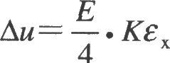
The choking phenomenon and the eliminating measure of operational amplifier circuit diagram
Published:2011/8/9 1:51:00 Author:Rebekka | Keyword: choking phenomenon , the eliminating measure, operational amplifier
When the integrated operational amplifier is choking, the amplifier circuit will lose the ability to zoom. It is equivalent to the signal which is blocked by the same op amp.For example, thevoltage follower will often occur choking as the width of the input and output voltage of the followeris the same. Its input signal width is ususlly large(when the follower is the output stage). If the op amp input stage bias voltage is less than the peak input signal peak, the peak of the input stage will turn to saturated. When the saturation occurs, the input and output voltage becomes the same phase, the negative feedback becomes a positive feedback. Obviously, the positive and negative feedback will make the input stage bein the saturated mode. The input signal cannot output normally, and the choking phenomenon will occur. (View)
View full Circuit Diagram | Comments | Reading(728)
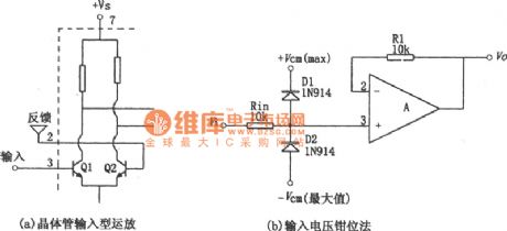
Input and output in-phase addition circuit composed of CF741
Published:2011/8/16 22:22:00 Author:Rebekka | Keyword: Input and output, in-phase addition
Input and output in-phase addition circuit composed of CF741 is shown as above. In the circuit, there are many parallel connecting input signals.Its output is multiple input signals linear superposition and it does not reverse. (View)
View full Circuit Diagram | Comments | Reading(751)
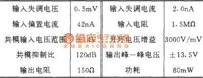
The gain adjustable addition circuit composed of CF725
Published:2011/8/16 22:26:00 Author:Rebekka | Keyword: gain adjustable addition
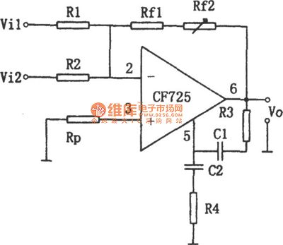
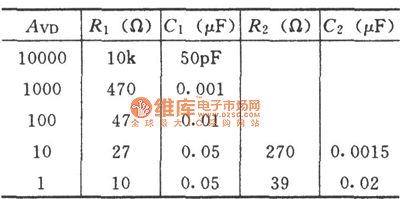
The circuit uses integrated operational amplifier CF725. The op amp is a monolithic precision operational amplifier with low power consumption, high voltage gain. It can be used for instrumentation etc.
The component values of frequency compensation network.
The typical main parameters of CF725.
(View)
View full Circuit Diagram | Comments | Reading(757)
Two functions four tones cycling burglar alarm circuit diagram
Published:2011/8/17 3:21:00 Author:Rebekka | Keyword: Two functions , four tones , cycling burglar alarm
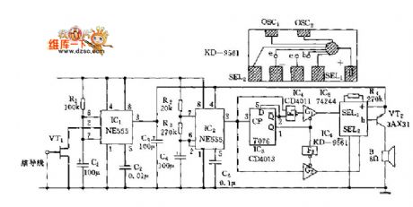
View full Circuit Diagram | Comments | Reading(668)
Wide Range Duty Cycle Grid Electrode Isolated Driving Circuit
Published:2011/8/18 5:46:00 Author: | Keyword: Wide, Duty Cycle, Grid, Electrode, Isolated, Driving
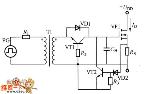
The picture shows the wide range duty cycle grid electrode isolated driving circuit by using the pulse transformer. In the circuit, the transformer T1's inductance and resistance R1 make up the differential circuit which would generate the power MOSFET's grid electrode driving voltage. If the transformer T1's secondary side generating the positive polar pulse (which means the high side is positive and the low side is negative), the VD1 would be conducted and charge the keeping capacitance CH and VF1's input capacitance Ciss. At this time the VT1's leakage current between grid electrode and the source electrode is very small. So even the input differencial pulse voltage is 0V, it would also keep the charging voltage. (View)
View full Circuit Diagram | Comments | Reading(909)
Grid Electrode Driving Circuit By Using Pulse Transformer
Published:2011/8/17 21:31:00 Author: | Keyword: Grid, Electrode, Driving, Pulse, Transformer
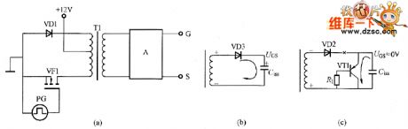
There are many advantages for the grid electrode driving circuit by using the pulse transformer. For example, the pulse transformer can make up a simple grid electrode isolated circuit and do not distinguish the high and low side driving circuit. The pulse transformer could also transmit the power, and the high-side driving circuit does not need the auxiliary power. The grid electrode driving conditions could be set freely.The high and side driving circuit could use the circuit with the same structure. In half-bridge circuit it could use the pulse transformer to make up the symmetrical drive circuit and so on.The picture shows the grid electrode driving circuit by using the pulse transformer. This circuit pulse transformer T1 could use the center tap method, and do the switching work by the transistor or power MOSFET. It is always used in the positive excitation conversion's switching power. (View)
View full Circuit Diagram | Comments | Reading(743)
Large-Power Full Bridge Circuit
Published:2011/8/17 0:41:00 Author: | Keyword: Large, Power, Full, Bridge
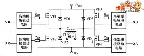
The large-power circuit is always using the full-bridge circuit which is shown in the picture. In the circuit, the VF1 is N-channel power MOSFET and its output voltage is twice of the half-bridge circuit. It the load is the same, its power would be 4 times of the power of the half-bridge circuit. So it is suitable for the large-power applications.
The picture shows the large-power full-bridge circuit.
In the full-bridge circuit, the two output ports are in floating mode. So if any port is connected with the power port, it would be the short circuit mode of the load, and the elements would be damaged. So it adds the isolated transformer T1. This transformer also has the function of impedance conversion, voltage boost and buck and so on. (View)
View full Circuit Diagram | Comments | Reading(785)
Grid Electrode Basic Driving Circuit
Published:2011/8/18 3:20:00 Author: | Keyword: Grid, Electrode, Basic, Driving
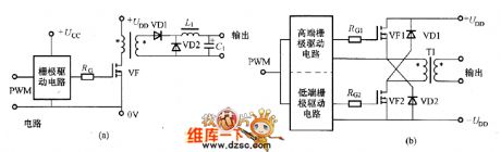
The power MOSFET's grid electrode driving circuit has different kinds of types according to the differences of the switching circuit. The picture shows the single-tube and dual-tube switching circuit. The picture (a) is a basic switching circuit composed of the power MOSFET whose the source electrode is connected to the ground. Its load could be resistance, inductance, switching transformer or DC motor and so on. The picture (b) is the swithing circuit composed of two power MOSFET and the VF1 and VF2 would be connected and disconnected working at the same time. Because there are clamp diodes VD1 and VD2 connecting in the power circuit, so the power MOSFET's withstand voltage needn't have the surplus capacity. (View)
View full Circuit Diagram | Comments | Reading(713)
The amplifier timed exposer circuit
Published:2011/8/15 21:57:00 Author: | Keyword: amplifier, timed exposer

The amplifier timed exposer can turn on the amplifier light, and the time is ranged from 1s to 20s, and it can also set the LED which flashes once per second, which is convenient for the dark room. The circuit consists of the comparator, timer and pulse timer. The comparator is used to estimate the exposing time. By adjusting VR1, the light volume on PCC1 can be tested. The timer is added on the non-inverting phase input terminal of IC1B by the VR3 adjusting Vref. When C2 is discharging, IC1B is outputting a high LEV, TR2 is conducting, the relay is working and the amplifying light is put through. (View)
View full Circuit Diagram | Comments | Reading(800)
| Pages:87/312 At 2081828384858687888990919293949596979899100Under 20 |
Circuit Categories
power supply circuit
Amplifier Circuit
Basic Circuit
LED and Light Circuit
Sensor Circuit
Signal Processing
Electrical Equipment Circuit
Control Circuit
Remote Control Circuit
A/D-D/A Converter Circuit
Audio Circuit
Measuring and Test Circuit
Communication Circuit
Computer-Related Circuit
555 Circuit
Automotive Circuit
Repairing Circuit