
Circuit Diagram
Index 1502
Phone busy indicator circuit2
Published:2011/7/6 19:58:00 Author:zj | Keyword: Phone busy indicator
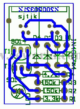
View full Circuit Diagram | Comments | Reading(564)
Telephone volume control circuit
Published:2011/7/20 2:34:00 Author:zj | Keyword: Telephone, volume control
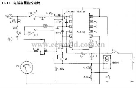
View full Circuit Diagram | Comments | Reading(814)
Long distance telephone ringing circuit
Published:2011/7/20 2:35:00 Author:zj | Keyword: Long distance, telephone ringing
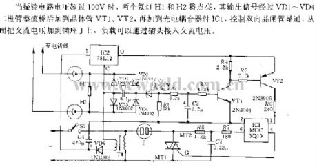
When voltage ofringing circuit is more than 100 V , the two neon light H1 and H2 will be lighted.The output signal will add to VT1、VT2 after rectifiering by VD1~VD4.Then it will add to Optoelectronic coupler IC1,control theconduction of TRIAC.Thus the ac voltage can be added to the socket J, the load will access ac voltagethrough the plug. (View)
View full Circuit Diagram | Comments | Reading(686)
LCl82 audio voltage control neon light pattern control circuit
Published:2011/5/10 7:41:00 Author:Nicole | Keyword: audio voltage control, neon light pattern
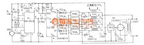
The control circuit is as shown. It consists of pickup sensor, sound control integrated circuit IC1, LC182 light control circuit, AC solid state relay and neon light drive circuit, AC depressurization rectifier circuit. Sensor BM is CRZ2 electret condenser microphone, it will transform the piched up sound singal into electrical signal. IC2 adopts special sound control integrated circuit BH-SK-II. Its chip contains three-level amplifier, shaper, frequency selection network, bistable trigger and drive circuit. The singal from sensor BM is added to input terminal 1 foot of SK-Ⅱsecond level amplifier through C1, after enlarged, it is outputed by 2 foot, and coupled to the input terminal 3 foot of SK-Ⅱthird level amplifier, it is enlarged and shaped again, it is fliped by triggering bistable state. SK-Ⅱhas two drive output terminals of 6 foot, 9 foot, it only uses output current terminal 9 foot as output. Outputed by SK-Ⅱ, The pulse singal is added to LC182 audio frequency singal input terminal UIN through C6. The sound(such as hand-clapping, beating) singal and the flipping of SK-Ⅱbistable state circuit is controlled by sensor BM, then to control the voltage control oscillator frequency inside SK-Ⅱ, it can realize voltage control to the cycle flashing frequency of color lamp. (View)
View full Circuit Diagram | Comments | Reading(822)
Telephone audio amplification and recording device
Published:2011/6/30 21:51:00 Author:zj | Keyword: Telephone, audio amplification, recording

View full Circuit Diagram | Comments | Reading(746)
Telephone repairing reference circuit
Published:2011/6/30 21:51:00 Author:zj | Keyword: Telephone, repairing
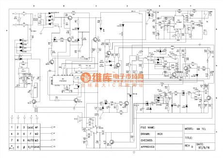
View full Circuit Diagram | Comments | Reading(1818)
Electric Water Heater Circuit 01
Published:2011/6/30 21:52:00 Author:zj | Keyword: Electric Water Heater, 01
View full Circuit Diagram | Comments | Reading(1274)
PC infrared remote control
Published:2011/6/30 21:52:00 Author:zj | Keyword: PC, infrared, remote control
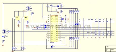
View full Circuit Diagram | Comments | Reading(1039)
Thermal furnace temperature regulating circuit
Published:2011/5/9 8:59:00 Author:Nicole | Keyword: furnace, temperature regulating
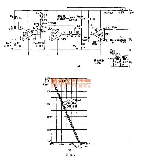
In general regulating circuit, the waste heat sensor is used as voltage divider, it is hard to obtain good linear relationship. The figure (a) may have linear relationship. A few waste heat devices can be controlled by a external control device, then it will produce a DC voltage which has relation with external condition, the value is between 0.91~1.43V. In figure (a), the input terminal 2 switch voltage U7 of operational amplifier OP2 is controlled by the attenuation ratio: RP3+R6/R7, it is about 0.91V, when the control voltage Us=0.
The figure (b) is a performance curve of circuit. When control voltage Us≦0.91V, hysteresis loop is about 20%, because the resistance R7 is in action in this region. (View)
View full Circuit Diagram | Comments | Reading(750)
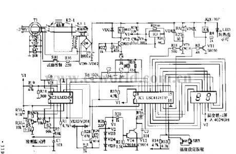
High limit of temperature animal bleating alarm and automatic ventilation cooling control circuit
Published:2011/5/16 3:50:00 Author:Nicole | Keyword: temperature, bleating alarm, ventilation cooling
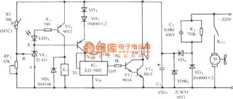
The circuit is as shown, it consists of upper temperature limit detection circuit, call alarm circuit, relay control fan lowering temperature circuit and AC depressurization power supply circuit. IC1 adopts CMOS large scale language integrated circuit KD-56021, it stores four kinds of animal sounds: sheep, cattle, chicken, dog. (View)
View full Circuit Diagram | Comments | Reading(603)
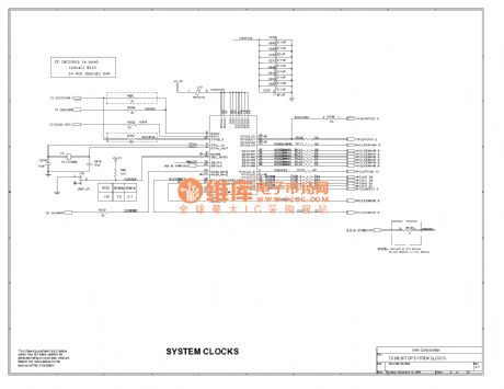
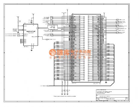
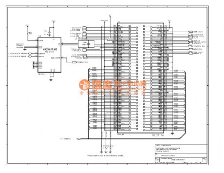
PC mainboard circuit 430TX_03
Published:2011/7/6 19:57:00 Author:zj | Keyword: PC mainboard
View full Circuit Diagram | Comments | Reading(540)
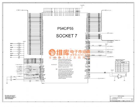
PC mainboard circuit 430TX_02
Published:2011/7/6 19:57:00 Author:zj | Keyword: PC mainboard
View full Circuit Diagram | Comments | Reading(532)
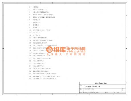
PC mainboard circuit 430TX_01
Published:2011/7/6 19:57:00 Author:zj | Keyword: PC mainboard
View full Circuit Diagram | Comments | Reading(525)
Full-bridge power convertor circuit diagram with increase output power
Published:2011/5/5 7:24:00 Author:Nicole | Keyword: Full-bridge power convertor
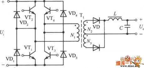
The two electrolytic capacitors of half-bridge converter circuit are changed to the other two high back pressure power transistors, and coupled with appropriate drive circuit then canformfull-bridge converter circuit, the figure is as shown. VT1, VT2, VT3, VT4 form 4 bridge arms. High frequency transformer T is connected between them. Relative VT1, VT4 and VT2, VT3 areinspired by the drive circuit, then theyturns onalternately, the DC input voltage into a high-frequency square-wave transform AC voltage. The course of working is the same as push-pull power converter circuit. Thus, when the high frequency transformer at work, the voltage of primary coil is considered to the supply voltage, it isone time ofthe half-bridge circuit output voltage, the pressure of each transistor remains at the supply voltage, twice the output power increases. If the current reaches half-bridge circuit, that means the current increases twice, then the output power can increase 4 times.
The main disadvantages of full-bridge circuit is that it needs 4 groups transistor base drive circuits which are insulative with each other, it enlarges the cost and complicates the control drive circuit.
(View)
View full Circuit Diagram | Comments | Reading(702)
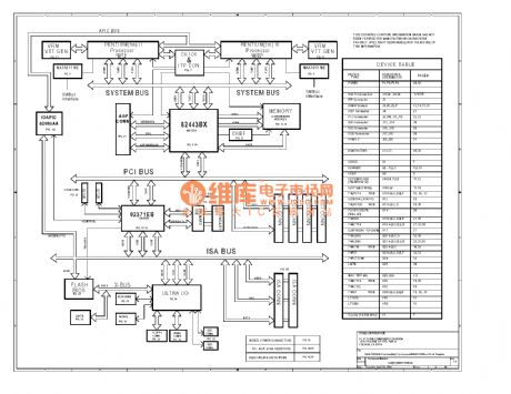
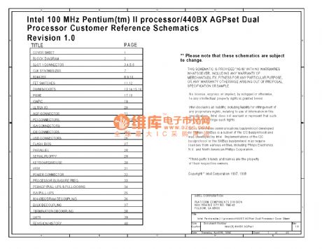
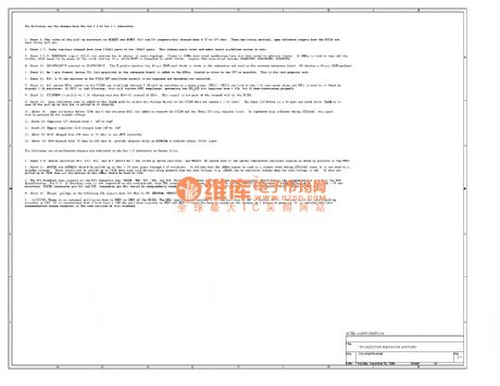
PC mainboard circuit 440BX-05
Published:2011/6/30 22:09:00 Author:zj | Keyword: PC mainboard, 440BX-05
View full Circuit Diagram | Comments | Reading(545)
PC mainboard circuit 440BX-04
Published:2011/6/30 22:09:00 Author:zj | Keyword: PC mainboard, 440BX-04

View full Circuit Diagram | Comments | Reading(520)
PC mainboard circuit 440BX-03
Published:2011/6/30 22:09:00 Author:zj | Keyword: PC mainboard, 440BX-03
View full Circuit Diagram | Comments | Reading(598)
PC mainboard circuit 440BX-02
Published:2011/6/30 22:10:00 Author:zj | Keyword: PC mainboard, 440BX-02
View full Circuit Diagram | Comments | Reading(685)
PC mainboard circuit 440BX-01
Published:2011/6/30 22:10:00 Author:zj | Keyword: PC mainboard, 440BX-01
View full Circuit Diagram | Comments | Reading(566)
PC mainboard circuit 430TX_30
Published:2011/6/30 22:10:00 Author:zj | Keyword: PC mainboard, 430TX_30
View full Circuit Diagram | Comments | Reading(502)
| Pages:1502/2234 At 2015011502150315041505150615071508150915101511151215131514151515161517151815191520Under 20 |
Circuit Categories
power supply circuit
Amplifier Circuit
Basic Circuit
LED and Light Circuit
Sensor Circuit
Signal Processing
Electrical Equipment Circuit
Control Circuit
Remote Control Circuit
A/D-D/A Converter Circuit
Audio Circuit
Measuring and Test Circuit
Communication Circuit
Computer-Related Circuit
555 Circuit
Automotive Circuit
Repairing Circuit