
Circuit Diagram
Index 1507
The battery voltage regulation charger circuit
Published:2011/7/18 1:56:00 Author:TaoXi | Keyword: battery, voltage, regulation, charger

As the figure 3-9 shows, the circuit uses the 555 as the comparator to control the charging current of the nickel cadmium battery.
The input of pin-5 is stabilized at 5.1V by the zener diode VD2 that can be used as the reference voltage. If the voltage of rechargeable battery is lower than 2.55V, the 555 will be triggered, the output of pin-3 will be the high level, and it charges the battery through the 100Ω resistance and the diode VD1. At this time the pin-7 will cut off, the LED turns on to indicate the charging state.
When the voltage of rechargeable battery is higher than the threshold voltage of pin-5, the timer will reset to stop the charging, pin-7 will conduct and the LED will turn off. The threshold voltage can be set by the fine-tuning resistance RP2.
(View)
View full Circuit Diagram | Comments | Reading(801)
Long interval timer circuit
Published:2011/7/17 1:55:00 Author:Fiona | Keyword: Long interval, timer
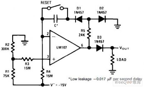
Long interval timer circuit is shown as above:
(View)
View full Circuit Diagram | Comments | Reading(1528)
The charger with the simple circuit
Published:2011/7/18 0:57:00 Author:TaoXi | Keyword: charger, simple circuit
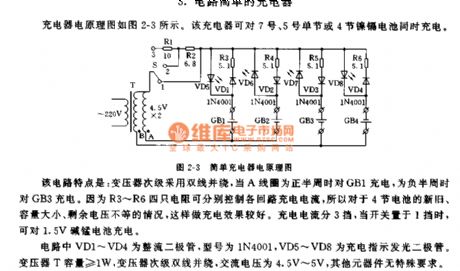
The charging principle diagram of this charger is as shown in figure 2-3. This charger can charge the no.5 or no.7 single or four nickel cadmium batteries synchronously.
The features of this circuit: the subprime stage of the transformer uses the bifilar winding, when the coil A is in the positive half cycle, it charges the GB1, when the coil A is in the negative half cycle, it charges GB3. The charging current has three stages, when the switch is in the 1 stage, it can charge the 1.5V alkaline battery. The VD1-VD4 are the rectifier diode, the model is 1N4001, the VD5-VD8 is the LED charging indicator. The capacity of the transformer T >/=1W, the transformer secondary stage is the bifilar winding, the AC voltage is 4.5V-5V.
(View)
View full Circuit Diagram | Comments | Reading(723)
Rapid zeropassage detector circuit
Published:2011/7/17 1:53:00 Author:Fiona | Keyword: zeropassage, detector
Rapid zeropassage detector circuit is shown as above:
(View)
View full Circuit Diagram | Comments | Reading(619)
Voltage regulation, charging, inverter three-function instrument circuit
Published:2011/7/17 22:29:00 Author:TaoXi | Keyword: Voltage regulation, charging, inverter, three-function, instrument
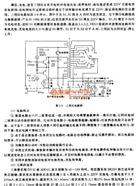
The voltage regulation, charging, inverter three-function instrument can charge the battery when there is the city electricity, When the power is outage, the battery inverts the 220V AC for the household appliances, when the grid voltage is too high or too low, you can adjust the output voltage to 220V manually to ensure the safety of the electric equipments. The circuit of the three-function instrument is as shown in figure 3-6. In this figure, when the switches S1 and S2 are in the A position, the circuit is in the inverter status. The left part of the circuit forms the self-excited oscillator to produce the 50Hz square wave, and this wave is boosted by the transformer and adjusted by S3 to be the 220V output. When the S1 and S2 are in the B position, the circuit is in the charging state.
(View)
View full Circuit Diagram | Comments | Reading(688)
Simple type nickel cadmium battery charger
Published:2011/7/15 4:22:00 Author:TaoXi | Keyword: Simple type, nickel cadmium battery, charger

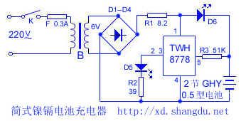
If you open the switch K, the 220V AC city electricity will be transformed by the transformer B, then the current is rectified by D1-D4 to charge the two GNY0.5 type battery (Number five nickel cadmium battery), the current is 500mA. The light of D6 means it is charging, at this time, the open voltage of the TWH8778 switching integrated circuit's control electrode pin-5 is lower than 1.6V, the circuit can not be conducted, so D5 will not turn on. As the continuation of the charge, the charging current of the GNY battery decreases gradually, the port voltage of the battery increases gradually, the voltage of the TWH8778's control electrode pin-5 increases gradually too, when the voltage is equal to 1.6V, the circuit conducts, D5 turns on to indicate that the battery is full.
(View)
View full Circuit Diagram | Comments | Reading(652)
Piezoelectric transducer of amplifier circuit
Published:2011/7/17 1:52:00 Author:Fiona | Keyword: Piezoelectric transducer, amplifier
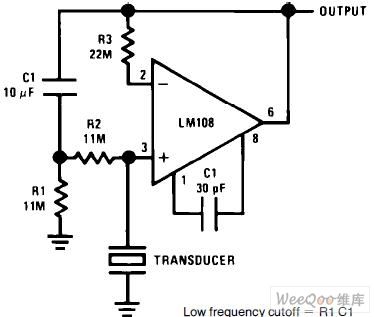
Piezoelectric transducer of amplifier circuit is shown as above:
(View)
View full Circuit Diagram | Comments | Reading(5810)
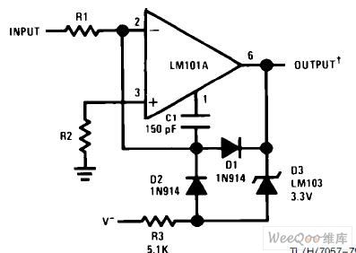
Low drift peak detector circuit
Published:2011/7/17 1:50:00 Author:Fiona | Keyword: Low drift, detector
Low drift peak detector circuit is shown as above:
(View)
View full Circuit Diagram | Comments | Reading(6119)
Simple programmable charger circuit
Published:2011/7/15 3:54:00 Author:TaoXi | Keyword: Simple, programmable charger
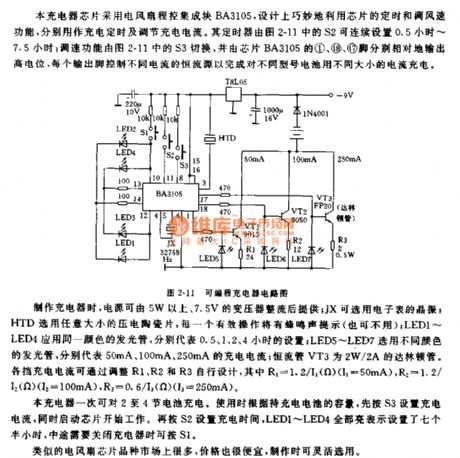
This charger uses the electric fan program control manifold block BA3105, it masterly uses the timing and wind speed regulating function of the chip, and the current can be used as the charging timing current and the adjustment charging current. The timer can be set to 0.5-7.5 hours by the S2 which is as shown in figure 2-11; the speed adjustment function is switched by S3 of the figure 2-11, and the pin-1, pin-18 and pin-17 relatively output the high level respectively, every output pin controls different constant current source.
When you are making the charger, the power can be supplied by 5W, 7.5V transformer.
(View)
View full Circuit Diagram | Comments | Reading(658)
Analog multiplier circuit
Published:2011/7/17 1:47:00 Author:Fiona | Keyword: Analog multiplier
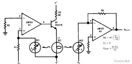
Analog multiplier circuit is shown as a bove:
(View)
View full Circuit Diagram | Comments | Reading(1459)
Accurate 12V storage battery automatic charger circuit
Published:2011/7/15 3:24:00 Author:TaoXi | Keyword: Accurate, 12V, storage battery, automatic charger

The principle diagram is as shown in figure 4-25, the secondary stage of the transformer is divided into two groups, L1 group is responsible for the charging, the light of LED1 means the rectifier power supply operating is normal. VS1 unidirectional thyristor is 6A, it uses the phase-shifting trigger circuit, you can change the phase angle by adjusting RP1 (change the charging current which flows through the VS1). The VS2 two-way thyristor is the passage-channel switch of the phase shifting trigger circuit. The L2 group is rectified, filted and stabilized to supply power to the IC1 to produce the trigger signal for the VS2, so VS2 is used as the phase shifting trigger circuit of VS1; on the other hand, it supplies to IC2 as the voltage comparator power supply.
(View)
View full Circuit Diagram | Comments | Reading(795)
Fast half wave rectifier circuit
Published:2011/7/17 1:45:00 Author:Fiona | Keyword: half wave, rectifier
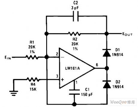
Fast half wave rectifier circuit is shown as above:
(View)
View full Circuit Diagram | Comments | Reading(1168)
Automatic charger circuit with the discharging function
Published:2011/7/15 2:34:00 Author:TaoXi | Keyword: Automatic charger, discharging function
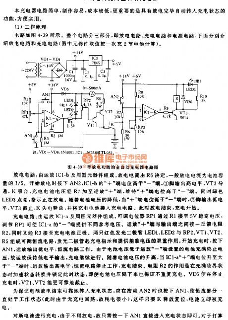
This ciruit is simple and easy to make, the cost is low, and it has the function of charging status automatic conversion.
Operating principle
The circuit is as shown in figure 4-39. The whole circuit is divided into three parts: the discharging circuit, the charging circuit and the power supply circuit. The charging circuit and the discharging circuit are introduced in this article.
The discharging circuit is composed of the op-amp IC1-b and the external components. The discharging current is decided by R6, the general discharge current is 1/5 of the battery capacity.
The charging circuit is composed of the op-amp IC1-a and the external components.
(View)
View full Circuit Diagram | Comments | Reading(653)
Precise AC and DC converter circuit
Published:2011/7/17 1:42:00 Author:Fiona | Keyword: AC and DC converter
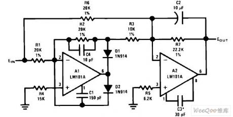
Precise AC and DC converter circuit is shown as above:
(View)
View full Circuit Diagram | Comments | Reading(851)
Low power integrated circuit test circuit
Published:2011/7/17 1:40:00 Author:Fiona | Keyword: Low power, test
Low power integrated circuit test circuit is shown as above:
(View)
View full Circuit Diagram | Comments | Reading(663)
Differential input instrumentation amplifier circuit
Published:2011/7/17 1:37:00 Author:Fiona | Keyword: differential input, instrumentation amplifier
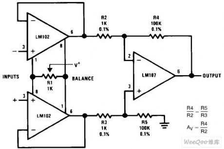
Differential input instrumentation amplifier circuit is shown as above:
(View)
View full Circuit Diagram | Comments | Reading(1098)
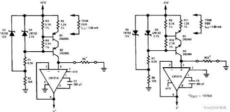
Variable gain differential input instrumentation amplifier circuit
Published:2011/7/17 1:36:00 Author:Fiona | Keyword: differential input, instrumentation amplifier
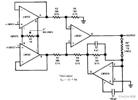
Variable gain differential input instrumentation amplifier circuit is shown as above:
(View)
View full Circuit Diagram | Comments | Reading(1937)
Simple charger circuit with the activation function
Published:2011/7/15 2:21:00 Author:TaoXi | Keyword: Simple charger, activation function
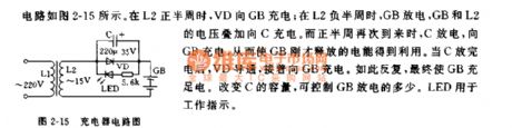
The circuit is as shown in figure 2-15. When L2 is in the positive half cycle, VD charges the GB; when L2 is in the negative half cycle, GB discharges, the voltage of GB and L2 are superimposed to charge C. When the positive half cycle comes again, the C discharges to charge the GB, so the power which is released by GB is utilized. When C is discharged, VD conducts to charge the GB. So repeatedly, the GB is fully charged. You can control the discharging of GB by change the capacity of C. The LED can be used in the working indication.
(View)
View full Circuit Diagram | Comments | Reading(673)
The motorcycle anti-theft alarm (2)
Published:2011/7/19 19:21:00 Author:TaoXi | Keyword: motorcycle, anti-theft, alarm
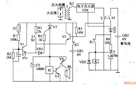
The multi-function motorcycle anti-theft alarm is introduced in this article, and it can be used in the anti-theft applications of all the two-wheel motorcycles.
The principle of the circuit
The motorcycle anti-theft alarm circuit is composed of the mobile delay alarm circuit, the ignition switch ground wire break alarm circuit, the right cover vandal resistant alarm circuit, the control circuit, the alarm signal generating circuit and the power-saving circuit, as the figure 7-85 shows.
The mobile delay alarm circuit is composed of the mercury switch Sl, the resistors Rl and R2, the delay capacitor Cl and the transistor Vl.etc.
(View)
View full Circuit Diagram | Comments | Reading(2396)
Battery charging regulator circuit
Published:2011/7/18 2:57:00 Author:TaoXi | Keyword: Battery, charging, regulator

This circuit uses the PHILIPS TEA1100 chip to charge the Nickel cadmium battery rapidly and effectively with the incremental peak principle. The circuit is as shown in figure 3-1.
The incremental peak regulator can detect and judge the change of the battery voltage: if the voltage of pin-7 decreases 1% or more of the average maximum value, the charging will continue. The voltage of pin-7 must be in the range of 0.385V-3.85V, the voltage dividers R4 and R5 can be used to supply the voltage that is in this range. The values of R4 and R5 can be ensured by this formula: R4/(R4+R5)>0.35n. The charging current Io=1.25R10/R8IIR9)R2, the charging time t0=226X0.93XR2XC3. When the circuit does not detect the maximum voltage value, the circuit will stop charging after the time of T0.
(View)
View full Circuit Diagram | Comments | Reading(1178)
| Pages:1507/2234 At 2015011502150315041505150615071508150915101511151215131514151515161517151815191520Under 20 |
Circuit Categories
power supply circuit
Amplifier Circuit
Basic Circuit
LED and Light Circuit
Sensor Circuit
Signal Processing
Electrical Equipment Circuit
Control Circuit
Remote Control Circuit
A/D-D/A Converter Circuit
Audio Circuit
Measuring and Test Circuit
Communication Circuit
Computer-Related Circuit
555 Circuit
Automotive Circuit
Repairing Circuit