
Circuit Diagram
Index 1501
Control AC load interface circuit
Published:2011/5/12 2:18:00 Author:Nicole | Keyword: control AC load, interface
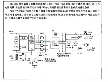
MC6820 external interface converter drives NAND gate 7400, 7400 output singal is fed to MOC3011 photoelectric isolator, it controls three terminal TRIAC which controls AC resistance load or AC inductive load.
To connect transistor timing circuit on the second input terminal of 7400 NAND gate , the TRIAC is on conduction only when the AC input voltage pass zero point. It can delay the usefil time of incandescent lamp, and reduce surge current to attack three terminal TRIAC, and decrease the back-EMF produced by load switch. (View)
View full Circuit Diagram | Comments | Reading(883)
High sensitivity sound snoop device
Published:2011/7/17 20:25:00 Author:zj | Keyword: High sensitivity, sound snoop device
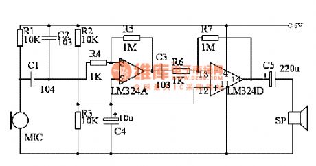
Working principle
The circuit is shown above.Microphone which is put in a special bobbinrecieves sound from certain direction(Other directions are inhibited). Sound is sent into amplifier. The amplifier is composed of two poles. Using it you can hear weak sound from far away.LM324 is integrated by four operational amplifier. Here just uses A&D. The connection method can refer to the diagram. (View)
View full Circuit Diagram | Comments | Reading(2761)
High voltage pulse generator circuit
Published:2011/5/11 8:52:00 Author:Nicole | Keyword: pulse generator
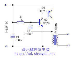
The figure is as shown, it uses 6V~12V DC power supply to produce a high voltage pulse. The oscillator is composed of triode Q1, Q2, it will produce a 3Hz DC pulse voltage, and it is imported a primary coil with 6V:240V, when the pulse is ended, it will produce a high voltage on the primary coil of transformer. The repetition rate of pulse depends on C2, R1. This circuit is used for truncheon, it can adopt lead-acid battery. (View)
View full Circuit Diagram | Comments | Reading(5380)
DAC667 basic connection and output voltage set up
Published:2011/7/17 20:12:00 Author:zj | Keyword: basic connection, output voltage, set up

View full Circuit Diagram | Comments | Reading(568)
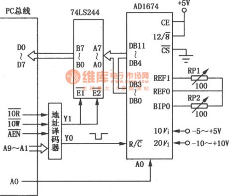
AD1674 and PC connection diagram
Published:2011/7/17 20:10:00 Author:zj | Keyword: PC, connection diagram
View full Circuit Diagram | Comments | Reading(817)
ICL7106 constitutes a micropower thermometer
Published:2011/7/20 2:38:00 Author:zj | Keyword: micropower thermometer
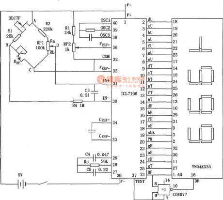
View full Circuit Diagram | Comments | Reading(6080)
Dual band modem composed of NE561B
Published:2011/7/20 2:39:00 Author:zj | Keyword: Dual band modem
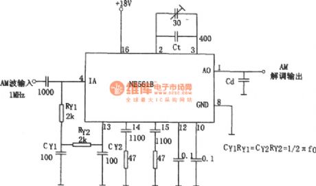
As the diagram shows it is a dual band modem composed of NE561B. The input modulation signal carrier frequency of the circuit f0=1MHz. When AM modulation signal adds to multiplier input terminal it adds to phase detection circuit by Rv1, CY1, RY2 and CY2 too. And it fixes the PLL VCO frequency on f0. (View)
View full Circuit Diagram | Comments | Reading(885)
Integration orthogonal detector circuit used in LED
Published:2011/5/11 8:52:00 Author:Nicole | Keyword: detector, LED
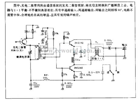
In figure, photodiode array is irradiated by LED of communication system, converting the optical information into broadcast band. The circuit is similar to 1:1 balance-disbalance converter, it has single-channel input, two-channel output, the phase shift between two output is 90 degrees. This circuit does not require neutralizing, it can give high gain reasonably and has low noise. (View)
View full Circuit Diagram | Comments | Reading(716)
Pointed pulse detection circuit
Published:2011/5/11 8:48:00 Author:Nicole | Keyword: pointed pulse, detection
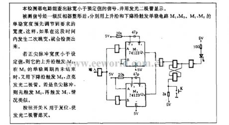
This detector circuit can detect the singal,the pulse width of this singalis smaller than the predetermined value, and displayed by LED.
After plastic by primar inverter, the tested signal uses rising edge and falling edge to trigger monostable circuit M1, M2. The monostable width of M1, M2 is adjusted to requested previously, so if it occurs second jumping, it will be detected.
If the positive pointed pulse width is smaller than set value, its rising edge trigger M1, when the monostable cycle of M1 is not finished,M2 is triggered by the falling edge, LED is lighted up. If it is negative pointed pulse, triggering M2 first, then trigger M1, the situation is similar.
The push-button switch K is used to reset, and to put out LED. (View)
View full Circuit Diagram | Comments | Reading(725)
Wiretapping amplifier circuit
Published:2011/6/29 3:08:00 Author:zj | Keyword: Wiretapping, amplifier
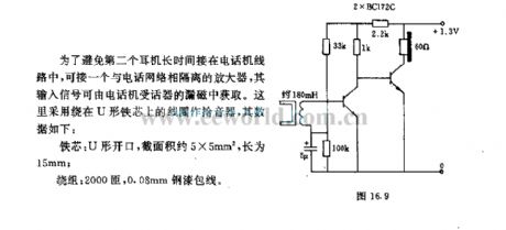
In order to avoidthat the second headset connects tothe telephone line for a long time,it can access in an isolated amplifier from the telephone network , the input signal can be obtained by the magnetic flux leakage of the telephone receiver.It usescoil around the U-shaped core for the pickuper, the data are as follows:
Core:U shaped port,the Cross-sectional area is about 5mm*5mm,the lenth is 15mm;
Winding:2000 turns,0.08mm steel wire. (View)
View full Circuit Diagram | Comments | Reading(847)
Light change detector drive relay circuit
Published:2011/5/11 8:45:00 Author:Nicole | Keyword: detector drive, relay
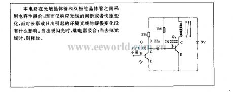
This circuit adopts electric capacity coupling between phototransistor and bipolar transistor, so it only has influence on the intermission or fast change of light, it has no effect on the slow change of ambient light produced by cloud or sunrise. When there is flashing, the relay pulls in; and if there is no light, it will release. (View)
View full Circuit Diagram | Comments | Reading(650)
Optical communication receiving circuit
Published:2011/5/11 8:44:00 Author:Nicole | Keyword: optical communication receiving
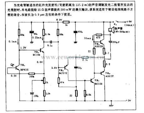
When the phototube is shined by the light which is produced by proper sound modulation LED of IR light transmitter(the transmitting distance is 137.2m), this circuit can provide 15Ω loudspeaker with 500mW maximum output. This system is suitable for the occasion where's difficult to install the electric wire, and it can be used when the wave length is about 0.9μm. (View)
View full Circuit Diagram | Comments | Reading(1354)
Optical pulse receiving circuit
Published:2011/5/11 8:41:00 Author:Nicole | Keyword: optical pulse
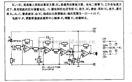
IC1~IC3 are high input resistance operational amplifier, IC4 is common operational amplifier. Photodiode D1 works with current, it has higher reverse bias voltage. The light signal received by D1 is amplified by IC1, filtered by IC2, amplified by IC3 again, then rectifier filtered by D2, R8, C4, outputed by comparator composed of IC4, its output range is -15~+15V.
In figure, P1 adjusts the middle frequency of bandpass filter, P2 adjusts the flipping point of IC4. (View)
View full Circuit Diagram | Comments | Reading(1461)
Photosensitization
Published:2011/5/11 8:37:00 Author:Nicole | Keyword: photosensitization
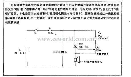
The cadmium sulfide photocell of thyristor trigger circuit is sensitive to the flashing in dark room and it is connected to relaxation oscillator, it leads to the loudspeaker souds out alarm, its alarm frequency increases with the increasing of the light density. When it is no flashing, R2 will be lower than the threshold value after adjusting. When this circuit is used for firelight alarming, it should use cadmium selenide to replace PC1, because cadmium selenide is sensitive to near infrared ray; when this circuit is use to heat alarm, because the spectrum is further expanded to far infrared band, so it should use pbs photocell due to it is sensitive to far infrared ray. (View)
View full Circuit Diagram | Comments | Reading(617)
Output record circuit of photoelectric multiplier
Published:2011/5/11 8:26:00 Author:Nicole | Keyword: output record, photoelectric multiplier
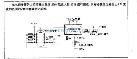
The large range output data of opto-electrical multiplier is fed by logarithmic amplifier 4351, the data is compressed into the range of ±5V DC, then it is fed to tape recorder. (View)
View full Circuit Diagram | Comments | Reading(635)
Circuit diagram: fat analyzer circuit diagram _ page _3
Published:2011/6/30 21:49:00 Author:zj | Keyword: fat analyzer, page _3
View full Circuit Diagram | Comments | Reading(1254)
Circuit diagram: fat analyzer circuit diagram _ page _4
Published:2011/6/30 21:49:00 Author:zj | Keyword: fat analyzer, page _4
View full Circuit Diagram | Comments | Reading(671)
Photoelectric lighting circuit
Published:2011/5/11 8:17:00 Author:Nicole | Keyword: photoelectric lighting circuit
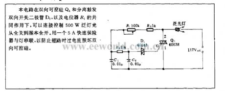
Under the action of TRIAC Q1 and separation trigger bidirectional switching diode D1 and potentiometer R1, this circuit can connect and control 500W light from all off to all on. 5A fast safety device is series connected with light, it can prevent TRIAC from damaging due to the short circuit. (View)
View full Circuit Diagram | Comments | Reading(711)
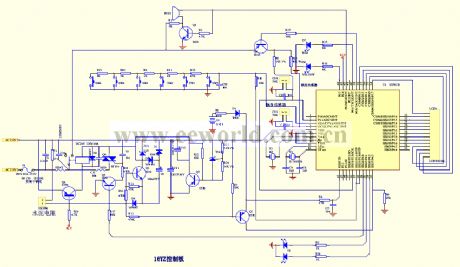
Rice cooker Circuit diagram 04
Published:2011/6/30 21:50:00 Author:zj | Keyword: Rice cooker
View full Circuit Diagram | Comments | Reading(1641)
Optical receiver circuit
Published:2011/5/10 8:02:00 Author:Nicole | Keyword: Optical receiver
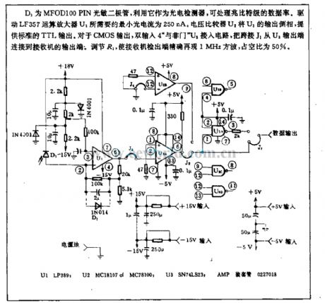
D1 is MFOD100 PIN photosensitive diode, using it as photodetector can deal with the data rate of Megabits Mb. The minimum photocurrent is 250nA which is needed by driving LF357 operation amplifier U1. U1's output is reversed phase by voltage comparator U2, it can provide standard TTL output. For CMOS output, double input 4 NAND gate U3 is connected into circuit, the bridge connection J1 is connected from U2 output terminal to receiver output terminal. To adjust R1, to make receiver take-off terminal accurate reappearance 1MHz square wave, the duty ratio is 50%. (View)
View full Circuit Diagram | Comments | Reading(742)
| Pages:1501/2234 At 2015011502150315041505150615071508150915101511151215131514151515161517151815191520Under 20 |
Circuit Categories
power supply circuit
Amplifier Circuit
Basic Circuit
LED and Light Circuit
Sensor Circuit
Signal Processing
Electrical Equipment Circuit
Control Circuit
Remote Control Circuit
A/D-D/A Converter Circuit
Audio Circuit
Measuring and Test Circuit
Communication Circuit
Computer-Related Circuit
555 Circuit
Automotive Circuit
Repairing Circuit