
Circuit Diagram
Index 858
OP_AMP_REGULATOR
Published:2009/7/10 0:03:00 Author:May


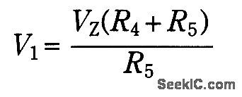


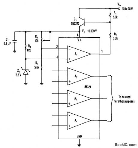
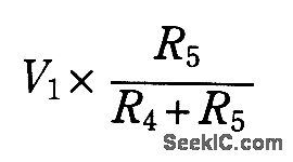


This op amp offers a straightforward method of developing a single-polarity stable voltage source (see the ftgure). Transistor Q1 gets a base drive through resistor R1, and conducts to develop a voltage(V1) across the IC's supply pins. Amp A1, R2, and Q1 form a positive-feedback closed loop, along with R3 and the zener diode. A1, R2, and Q1 also form a negative-feedback closed loop with R4 and R5.The effect of positive feedback is predominant as the noninverting input receives V1while the inverting input receives only: This happens until the zener comes into play. When the voltage at the inverting input exceeds the voltage at the noninverting input, A1's output takes away Q1's base current through R2, which reduces V1.Hence, an equilibrium condition is reached. Now:This circuit can source more than 30 mA. (View)
View full Circuit Diagram | Comments | Reading(1009)
WIRELESS_CONTROL
Published:2009/7/20 1:44:00 Author:Jessie
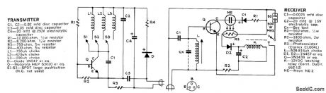
Choice of three lamps or appliances anywhere in house and garage, or even in neighboring home if on the same power transformer, can be turned on or off individually with three-channel transmitter that plugs into any wall outlet. Transmitter injects one of three tones (depending on button pushed) into house wiring. Receivers at locations of controlled de-vices are each tuned to one of carrier tones. Correct tone for receiver energizes neon lamp, and resulting light is picked up by photo resistor that energizes latching relay K for turning on controlled device. Relay is released by sending same tone again. Values of CX can be 0.005, 0.01, and 0.02μF, Adjust slug of L2 for each receiver so neon comes on when assigned tone for that receiver arrives.-W. J. Hawkins, Three-Channel Wireless Switch-Use It Anywhere, Popular Science, Sept. 1973, p 98-99 and 121. (View)
View full Circuit Diagram | Comments | Reading(874)
CURRENT_TO_FREQUENCY_CONVERTER
Published:2009/7/10 Author:May
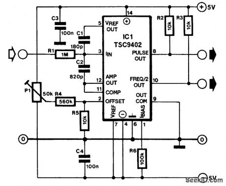

Teledyne Semiconductor's Type TSC9402 IC is eminently suitable as an mexpenstve current-to-fre-quency converter. The maximum input current of the design shown in the diagram is 10 μA (input voltage range is 10 mV to 10 V), while the output frequency range extends from 10 Hz to 10 kHz. The conversion factor is exactly 1 kHz/μA. The factor can be altered by changing the value of R1-as long as the maximum input current of 10 μA is not exceeded.
The circuit has two outputs. That at pin 8 is a short-duration pulse, whose rate is directly proportional to the input current; that zit pin 10 is a square wave of half the frequency of the pulse at pin 8.
Calibrating the circuit is fairly simple. Connect a frequency meter to pin 8 (preferably one that can read tenths of a hertz) and connect a voltage of exactly 10 mV to the input (check with an accurate millivoltmeter). Adjust Pl to obtain an output of exactly 10 Hz. Next, connect a signal of exactly 10 V to the input and check that the output signal has a frequency of 10 kHz. If this frequency cannot be attained, shunt C1 with a small trimmer or replace R1 by a resistor of 820 kΩ and a preset of 250 kΩ.
The circuit may be adapted to individual requirements with the aid of:
(View)
View full Circuit Diagram | Comments | Reading(1796)
PRECISION_FREQUENCY_GENERATOR
Published:2009/7/20 1:43:00 Author:Jessie

Provides 440 cps at 115 v for timing motor of engraved-foil flight recorder. Uses saturating-transformer oscillator and auxiliary regulating circuits to maintain precise voltage and frequency.-H. E. Schauwecker, Dote Recorder for Airplane Flight Analysis, Electronics, 33:48, p 118-120. (View)
View full Circuit Diagram | Comments | Reading(737)
POWER_SAVING_INTERMITTENT_CONVERTER
Published:2009/7/9 23:58:00 Author:May
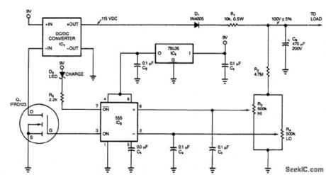
This circuit switches its dc/dc converter, IC1, off whenever the large filter capacitor, C6, has sufficient charge to power the load. This particular circuit uses a dc/dc converter that produces 115 Vdc from a 9-Vdc input; you can tailor the circuit to suit other converters. The heart of the circuit is a 555 timer configured as a dual-limit comparator. Thus, the 555 turns the converter on or off, depending on the voltage across CG. The 555's complementary output lights the charge LED when the FET is on.
Initially, the voltage on CG is zero, and the 555's output turns on the FET, Q1, in turn, enabling the converter to run, which charges C6. When the voltage on the capacitor reaches the value set by R3, the 555 turns the converter off. Then, C6 slowly discharges into the combined load of the voltage divider (R2, R3, and R4) and the reverse-biased blocking diode, D1.
When the voltage falls below 1/3 VCC, the 555 restarts the dc/dc converter. If this circuit powers a load that periodically goes into a zero-power, shutdown mode, the 555 switches the dc/dc converter on full time whenever the load kicks in.
When the supply voltage falls below 7.5 V, the output of the converter is no longer high enough to charge, the LED doesn't light. The circuit uses 205 mA when the converter is on and 10 mA when the converter is off. The duty cycle comprises a 5-s ON period, a 150-s OFF period, and it represents a 92% power reduction. You can further reduce power consumption by removing the charge LED and using a CMOS 555 and a CMOS 78LO5 regulator. (View)
View full Circuit Diagram | Comments | Reading(1124)
MULTIPLYING_PRECISE_COMMUTATING_AMP
Published:2009/7/9 23:55:00 Author:May
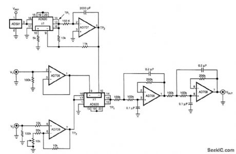
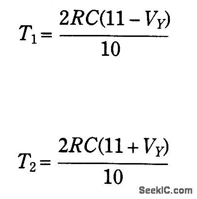
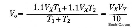
By using a pulse-width-height modulation technique, this circuit implements a 0.015%-accurate multi-plier. The circuit's output equals VXVY/10. An AD581 voltage reference, an AD630 commutating amplifier, and an integrator comprising an AD707 op amp, 2000-pF capacitor, and 150-kΩ resistor first generate a precision triangle wave. For a given state of the AD630's output (+VREF at TP1, for example) the integra-tor ramps until its output reaches -11V. Then, TP) changes state and the integrator begins ramping toward +11V. The triangle wave's period is 4.4RC or 1.32ms, where R and C are the values of the integrator components.
The circuit uses a second AD630, driven by the variable VX to compare the triangle waveform at TP2 to the signal at VY The duty cycle, T1+T2, at the output of this second commutating amplifier is:
During T1, the voltage at TP4 equals -1.1VX. During the remaining period, T2, the pulse height will equal+1.1VX. VOUT is the average, obtained by low-pass filtering, of this T1 and T2 combined waveform and equals:
You can use a higher bandwidth filter and a higher carrier frequency to build a faster multiplier. (View)
View full Circuit Diagram | Comments | Reading(982)
FAST_BINARY_ADDING_CIRCUITS
Published:2009/7/9 23:50:00 Author:May
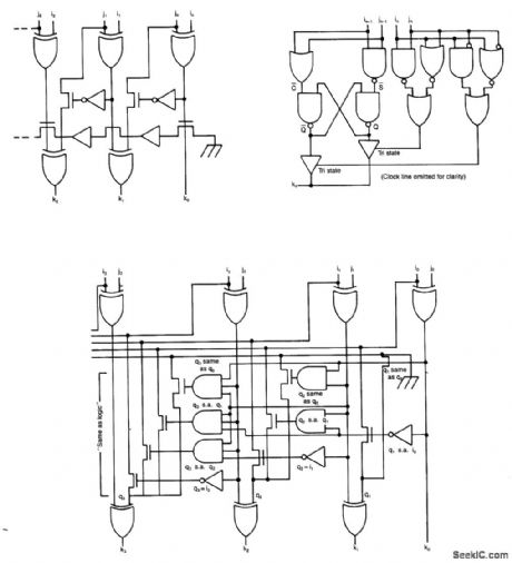
Some circuits that add binary numbers have problems with time delay caused by carry propagation.This has been partially solved by the carry look-ahead adder. However, because of the complexity of this scheme, the carry look-ahead logic usually covers no more than 4 bits, and a ripple carry is implemented between the carry look-ahead blocks.
The Daniels Adder avoids these problems by presenting a scheme where carry bits are not used at all in the process of binary addition. It is based on recognition patterns, which exist with the binary addition truth table.
The addition is described by the following two sets of equations:
if in-1=jn-1 qn=in-1if in-1=jn-1 qn=qn-1if in=jnkn=qnif in=jn kn=qn
with the boundary condition that q-1=0, where in,jn and kn are the bit of binary weight 2n (nth bit) of the addend, summand, and sum respectively, qn is an intermediate variable and qn is the inverse of qn.
The value of the sum is (depending upon in, and jn) either the same as or the inverse of (depending upon in-1 and jn-1) a0, a1, or the inverse of the (n-1)th bit of the sum. Figure 45-1(a) shows the logic diagram of the ripple through implementation of the adder.
Because each stage calculates whether its value of the intermediate variable qn is the same as the previous stage's value (qn-1) in parallel, it is possible to devise simple same as logic that does not have the complexity drawback of carry look-ahead logic and can be carried over any number of bits (Fig.45-1(b)). A 32-bit adder built in this way will result in 11-gate delays (no gate having more than 4 inputs).
Especially compact and efflcient is the pipelined implementation (Fig. 45-1(c)), which can produce the sum at a rate of 3-gate delays/bit.
The high-speed adder circuits can be used on gate arrays or full-custom ICs to implement fast calcula-tion of addresses or data values. Because of their compact nature, they also use less space on the silicon than conventional adders do. (View)
View full Circuit Diagram | Comments | Reading(1971)
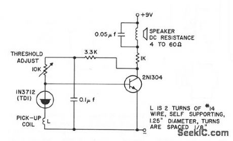
LIGHI_DETECTOR
Published:2009/7/9 23:50:00 Author:May
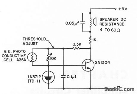
Gives 1,800-cps alarm tone when illumination on photocell exceeds predetermined level, which can be below 0.1 foot-candle near 5,500 angstroms.- Transistor Manual, Seventh Edition, Gemeral Electric Co., 1964, p 363. (View)
View full Circuit Diagram | Comments | Reading(754)
EFFICIENT_POWER_BOOSTER
Published:2009/7/9 23:50:00 Author:May

This power booster functions as a high-efficiency power multiplexer or, if you supply an external signal-source, as a high-power linear amplifier.
If you want to drive a load with a high-power square wave, the circuit simply draws power from two external power sources, V1 and V2, alternately. In this mode, the circuit's power-handling devices func-tion as switches, dissipating minimal power. The RC time constant of the integrator,IC1, determines the circuit's oscillation period.
If you supply an external drive waveform, the circuit functions as a linear amplifier,and,consequently, inherently dissipates varying portions of that power. The power amplifier is stable for gains ≥15.
Diodes D1 and D2 limit the FET's gate-voltage swing to less than 15 V. D3 is a dual Schottky diode that protects the FETs from short circuits between the two supplies, V1 and V2, through a FET's para-sitic diode. With D3 in place, you can choose either power channel for the higher voltage input. To drive the FETs, Q5 and Q6, at switching frequencies greater than 1 KHz, you will have to use gate drivers for them. (View)
View full Circuit Diagram | Comments | Reading(714)
4_TO_20_mA_CURRENT_LOOP
Published:2009/7/9 23:49:00 Author:May
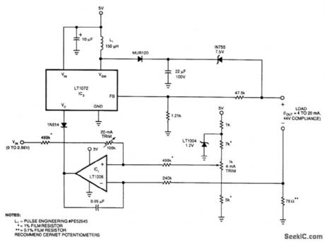
This 5-V circuit utilizesa servo-controlled dc/dc converter to generate the compliance voltage necessary for loop-current requirements. This circuit will drive 4 to 20 mA into loads as high as 2200Ω with 44 V of compliance. It is inherently short-circuit protected. A current source by definition limits current regardless of the load.
The circuit's input voltage and the 4-mA trim network determine 101's positive input voltage. IC1's output biases the LT1072 switching regulator's VC pin, The resistors connected to the regulator's feedback pin, BB, prevent the circuit output from running away in the event that the load opens up.
Normally, IC1 controls the loop. However, if the load opens, IC1 receives no feedback. Under this condition, the Fs pin becomes active when it equals 1.2 V and forces the loop to close locally around the regulator by activating IC2's internal amplifier. Thus, the circuit automatically changes from a current to a voltage regulator, thereby preventing excessive output voltages. (View)
View full Circuit Diagram | Comments | Reading(971)
LAMP_BURNOUT_ALARM
Published:2009/7/9 23:49:00 Author:May
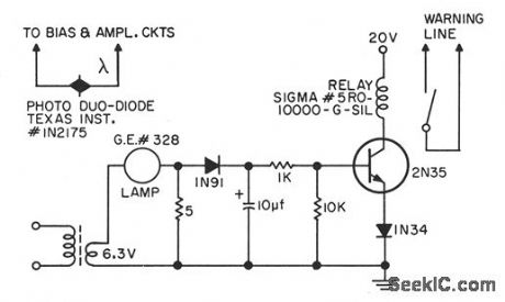
Used when photocells and lamps are employed to detect end of magnetic tape, lood point, or bad spot.Failure of lamp can cause serious trouble in magnetic tape handler. With circuit showm, when lamp burns out, transistor can no longer energize relay, and relay contact doses to actuate alarm at computer console.-J. E. Kienle and R. W. Wooldridge, Photocell Lamp Burnout Warning Circuit, EEE, 10:8, p 27-28. (View)
View full Circuit Diagram | Comments | Reading(905)
DIGITALLY_CONTROLLED_VOLTAGE_REFERENCE
Published:2009/7/9 23:45:00 Author:May
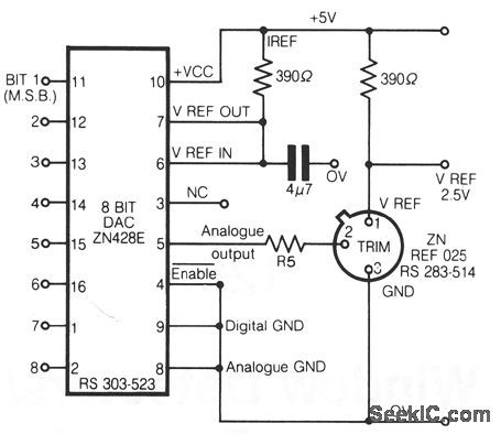
This circuit shows a simple method of achieving a voltage reference which can be trimmed using an 8-bit DAC with an on-chip voltage reference. The analogue output from the DAC drives the trim pin of the ZNREF025 via a resistor, RS. When RS = 0, this circuit will produce a trim range exceeding ± 5% of the nominal reference voltage. When RS is greater than zero, the trim range is reduced. It was found that after dividing the trim range by two, the needed value for RS was approximately 1 MΩ.The reference voltage of the ZNREF025 can be set to an accuracy determined by the trim range of the device itself and the accuracy of the DAC. Increasing RS reduces the percentage trim range and hence increases the effective voltage resolution. Other voltage references from the ZNREF series can be used with this circuit if other voltages are required. This voltage reference can be used to set the value of VREF to a much tighter tolerance, than the data sheet specification of ± 1%, in a much wider range of operating conditions. Applications could include any system with automatic self-calibration of instrumentation, such as in electronic weighing scales. (View)
View full Circuit Diagram | Comments | Reading(1138)
MULTIPLE_INPUT_ALARM
Published:2009/7/9 23:44:00 Author:May
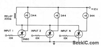
Any of several inputs will pull in common alarm relay, with corresponding lamp giving visual indication of triggered circuit. For higher-current laps, use 3N81 silicon controlled swilches.- Iransistor Manual, Seventh Edition, General Electric Co., 1964, p 425.
(View)
View full Circuit Diagram | Comments | Reading(1036)
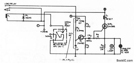
MISSING_PULSE_DETECTOR
Published:2009/7/9 23:44:00 Author:May

Warning light comes on to indicate occasional skipping of timing pulse or gate trigger having 20-pps rote, with durations ranging from 2 microsec to 30 millisec. Detector is triggered if interval between any two pulses exceeds 75 millisec, and must then be reset by pushbutton.-H.S. Reichard, Missing Pulse Detector, EEE, 10:6, p 35. (View)
View full Circuit Diagram | Comments | Reading(0)
PULSE_AND_D_C_MONITOR
Published:2009/7/9 23:42:00 Author:May
Indicates presence of continuous train of pulses, absence of one or more pulses in train, and dropout of d-c level beyond predetermined time interval. Uses controlled monostable mvbr. With d-c inputs, C2 is shorted. With values shown for R1 and C1, output occurs 1.07 millisec after last pulse.-Pulse and DC Monitor Circuit, Electronic Circuit Design Handbook, Mactier Pub. Corp., N.Y., p 201. (View)
View full Circuit Diagram | Comments | Reading(725)
200_MC_R_F_RADIATION_DETECTOR
Published:2009/7/9 23:41:00 Author:May
Gives 1,800-cps alarm tone when signal is picked up by coil or by small slot antenna serving as sensor.- Transislo r Manual, Seventh Edition, General Electric Co., 1964, p 363. (View)
View full Circuit Diagram | Comments | Reading(893)
NOISE_BLANKER
Published:2009/7/9 23:41:00 Author:May
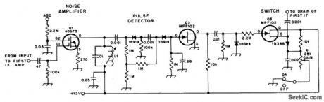
This nolse blanker takes a sample of IF input voltage, amplifies it, and drives a switch, The switch(when activated by a nolse pulse) adds a heavy load to the first IF stage and kills the gam for the pulseduration. (View)
View full Circuit Diagram | Comments | Reading(2082)
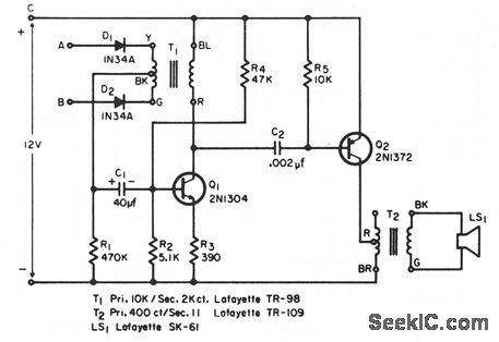
GYRO_FAULT_ALARM
Published:2009/7/9 23:40:00 Author:May
Circuit sounds alarm if gyro wheel is locked up, as indicated by input signed remaining at high current or voltage level for longer than preset interval.Circuit can also be used as pulse-level discrimincttor.-R. L. Sazpansky, Pulse-Level Discriminator and Fault Indicator, EEE, 13:8, p 68. (View)
View full Circuit Diagram | Comments | Reading(969)
DIFFERENTIA_L_VOLTAGE_ALARM
Published:2009/7/9 23:39:00 Author:May
Deleclor circuit with high sensitivity and stability, followed by audio ampliler, serves as differential voltage or current alarm. Input may be d-c or low-frequency a-c. Output is distinctive series of audio beeps or continuous tone, occurring only when preselected polarity unbalance is present at input.-C. E. Miller, Differentktl-Voltage or Current Alarm Circuit, EEE, 12:7, p 25. (View)
View full Circuit Diagram | Comments | Reading(930)
PROGRAMMABLE_SLOPE_INTEGRATOR
Published:2009/7/9 23:38:00 Author:May

By using analog swi,ch IH5009/IH5010 to select various capattors, a variable slope integrator can be had.If C3=2(C2) and C4=4(C2), seven different slopes can be obtained if binary informatlon is fed to pins 1, 7, and 8 of the analog switch. (View)
View full Circuit Diagram | Comments | Reading(967)
| Pages:858/2234 At 20841842843844845846847848849850851852853854855856857858859860Under 20 |
Circuit Categories
power supply circuit
Amplifier Circuit
Basic Circuit
LED and Light Circuit
Sensor Circuit
Signal Processing
Electrical Equipment Circuit
Control Circuit
Remote Control Circuit
A/D-D/A Converter Circuit
Audio Circuit
Measuring and Test Circuit
Communication Circuit
Computer-Related Circuit
555 Circuit
Automotive Circuit
Repairing Circuit