
Circuit Diagram
Index 845
Number_cruncher_interface_with_the_SC_MP_microprocessor
Published:2009/7/19 22:51:00 Author:Jessie
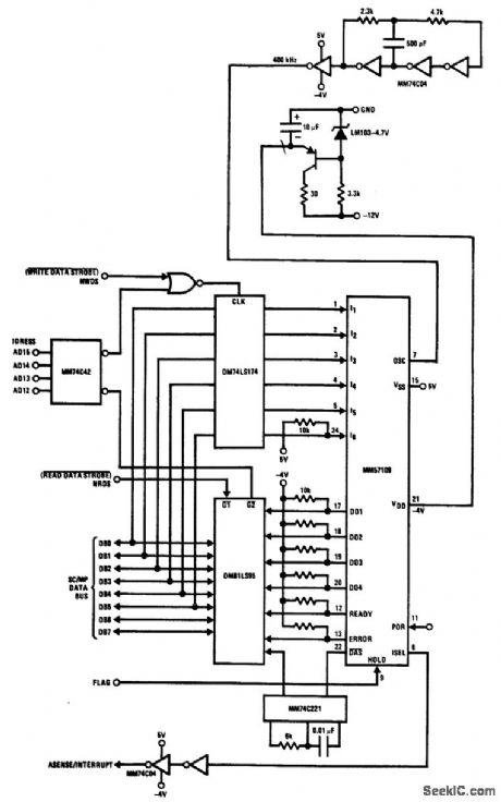
Number cruncher interface with the SC/MP microprocessor. The number cruncher unit (NCU) shown is an MM57109 (courtesy National Semiconductor Corporation). (View)
View full Circuit Diagram | Comments | Reading(1200)
METER_TESTER
Published:2009/7/10 2:13:00 Author:May
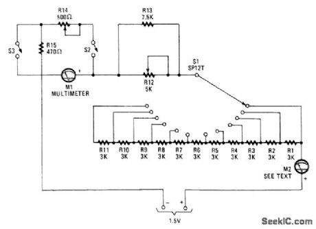
This unit uses switches and resistors to provide a number of current ranges. It allows you to test most of the meters available at surplus outlets, and without damaging the sensitive movements when you have no idea of internal resistance or full-scale current of the unit.
M1 is a multimeter set to measure current, and M2 is the meter-under-test. Starting with S1 set at the maximum resistance and S2 open, decrease the resistance setting of S1, fine tuning with R12, until M2 reads full scale. Then, read Ml. It will tell you the full-scale current for the unknown meter. As the meters are connected in series, the same current flows through both.
Now, close S2 and adjust R14 and R15 until M2 reads exactly mid-scale and M1 reads the same cur-rent as determined earlier to be the maximum current for M2. Half the current is flowing in M2 and half is going through R14 and R15. The voltage drop is the same across the meter and R14 and R15, because they're in parallel. Thus, the sum of the resistance of R14 and R15 is the same as the internal resistance of meter M2.
If the internal resistance of M2 is less than 470Ω, set R14 at maximum resistance and close S3. Read-just R14. Both R14 and R12 should be linear-taper potentiometers. (View)
View full Circuit Diagram | Comments | Reading(935)
TONE_SIGNAL_REJECTOR
Published:2009/7/19 22:49:00 Author:Jessie
Used to separate desired backscatter pulses from unwanted tone signals of interfering stations on same frequency. Negative-going portion of tone signal is rectified and used us slicer level for passing desired pulse, which rides on top of interfering tone.-K. Perry, Reducing Interference in Ionospheric Sounding, 33:22, Electronics, p 118-120. (View)
View full Circuit Diagram | Comments | Reading(659)
6_V_flasher
Published:2009/7/19 22:49:00 Author:Jessie

This circuit shows an LED flasher that uses an LM3909 with a 6-V supply. Notice that the circuit is similar to that of Fig. 12-43B, except that a 75-Ω resistor is required between pin 6 and the LED, a 3.9-kΩ resistor is used between pin 5 and pin 1, the 300-μF capacitor should be at least 3 V, and pin 5 receives +6V from the external source. The flashing rate remains at about 1 Hz.
Linear Applications Handbook. 1991. p 395 (View)
View full Circuit Diagram | Comments | Reading(922)
SINGLE_CHIP_MELODY_GENERATOR
Published:2009/7/10 2:13:00 Author:May
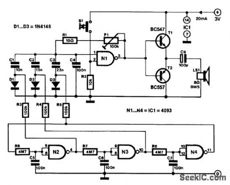
This melody generator, based on a 4093 CM0S Schmitt trigger, can be used in alarms, doorbells, and cars (audible reverse gear or lights-on indicator).Three of the four NAND gates in the 4093 are connected in series by RC networks. Oscillation is affected by feedback of the output signal of N4 to the input of N2. The logic-high levels produced by the cascaded gates in the oscillator circuit are used to bias one of associated diodes D1, D2, or D3). The relevant diode connects one of the frequency-determining capacitors (C1 through C3) to tone oscillator N1. The audio signal available when S1 is pressed is applied to complementary transistor pair (T1/T2) that drives the loudspeaker. The frequency of the emitted tone can be adjusted to individual taste with preset P1. (View)
View full Circuit Diagram | Comments | Reading(2508)
±24V_REGULATED_AND_±35V_UNREGULATED
Published:2009/7/19 22:48:00 Author:Jessie
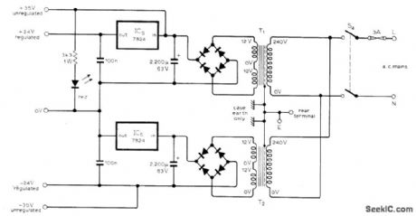
Developed for use with high-performance stereo preamp. Each IC regulator re quires about 7 cm2 of heatsink area. Red LED is TIL209 or equivalent.-D Self, Advanced Preamplifier Design Wireless World,Nov,1976 p41-46. (View)
View full Circuit Diagram | Comments | Reading(984)
AUDIO_FOR_A_M_F_M_PORTABLE
Published:2009/7/19 22:48:00 Author:Jessie

Overall power gain is 70 db, with audio output of 1 w at less than 10% distortion.-R. A. Santilli and H. Thanos, Portable Radio Uses Drift-Field Transistors, Electronics, 33:28, p 48-50. (View)
View full Circuit Diagram | Comments | Reading(650)
MICROPOWER_CLOCK
Published:2009/7/10 2:13:00 Author:May
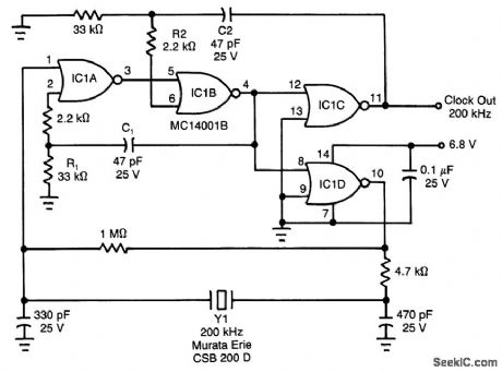
Although ceramic resonators are a good choice for low-power, low-frequency clock sources (if you can stand their 30-ppm temperature coefflcient), they have troublesome, spurious-resonance modes. This circuit rejects all but the resonator's fundamental mode. This clock circuit works from -40 to +80℃ and consumes only 2.8 mW.
The rising edge of resonator Y1 toggles IC1A low. ac-coupled positive feedback from IC1D via C1 and R1 immediately confirms this state change at IC1B so that Miller loading, harmonic components, or below-minimum rise times at IC1A cannot force IC1C to relapse to its previous state. This tactic also applies to resonator Y1's falling edge because IC1C, via CZ agd R2, holds ICIB high.
Choose time constants R1C1, and R2C2 to be equal and ranging from 60 to 75% of one-half of the clock's period. Ceramic capacitors (10% tolerance) with X7R dielectric work well. With these time constants, the logic will be locked and unavailable to the ceramic resonator until just before it executes a legitimate transition. IC1D and IC1C are in parallel to isolate the resonator from external loads and, more importantly, from C2. (View)
View full Circuit Diagram | Comments | Reading(0)
Teletypewriter_RS_232C_terminal_to_MC6850_ACIA_interface
Published:2009/7/19 22:47:00 Author:Jessie
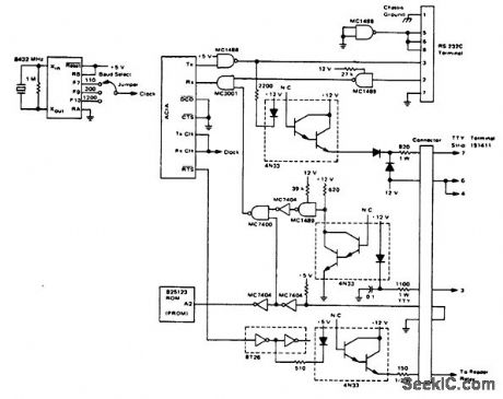
Teletypewriter/RS-232C terminal to MC6850 ACIA interface (courtesy Motorola Semiconductor Products Inc.). (View)
View full Circuit Diagram | Comments | Reading(1224)
REMOTE_GAIN_CONTROL
Published:2009/7/10 2:12:00 Author:May
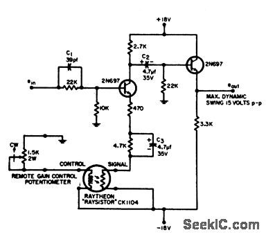
Permits adiusting gain of wideband amplifier over full range from maximum to zero with two-wire low-voltage line up to 1,000 feet long. Control and signal circuits are completely isolated.Components shown give maximum gain of l.-R. S. Young, Amplifer with Remote Gain Control, EEE, 12:8, p 71. (View)
View full Circuit Diagram | Comments | Reading(745)
THREE_TRANSISTOR_A_M_F_M_I_F_STRIP
Published:2009/7/19 22:46:00 Author:Jessie
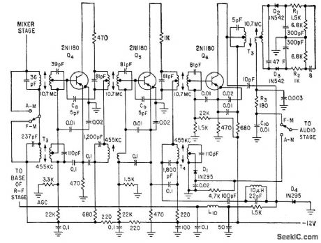
Used in a-m/f-m portable radio. Only two stages operate on a-m.-R. A. Santilli and H. Thanos, Portable Radio Uses Drift-Field Transistors, Electronics, 33:28, p 48-50. (View)
View full Circuit Diagram | Comments | Reading(655)
5V_AT_5A
Published:2009/7/19 22:46:00 Author:Jessie
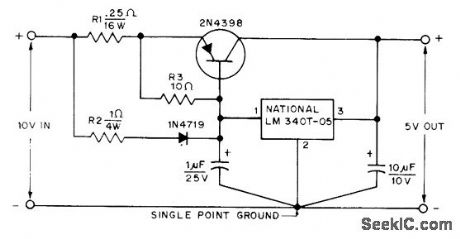
Current-sharing design provides short-circuit protection, safe-operating-area protection, and thermal shutdown. Typical load regulation is 1.4%.-W. R. Calbo, A High-Cur-rent, Low-Voltage Regulator for TTL Circuits, QST, Sept. 1975, p 44 (View)
View full Circuit Diagram | Comments | Reading(753)
HOLD_CURRENT_LIMITER
Published:2009/7/10 2:12:00 Author:May
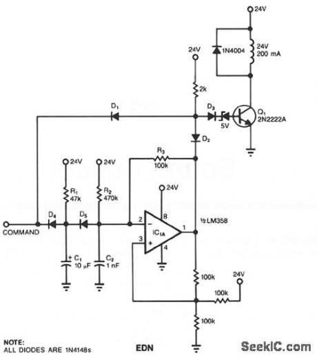
In many applications, a solenoid driver must ftrst briefly supply a large amount of pull-in current, which quickly actuates the solenoid. Thereafter, the driver must supply a much lower holding current to avoid burning the solenoid out. To avoid using the customary, cumbersome, large capacitors or power-wasting resistors, you can use the switch technique.As long as the input to the circuit is low, diode D1 holds Q1 off; a low input also prevents the op-amp circuit from oscillating. When the input reaches 24 V, Q1 switches on and pulls in the solenoid. Concurrently, D4 is back-biased, and C1 begins charging up. When C1 charges up, the op-amp circuit begins to oscillate, switching Q1 on and off.The time constant defmed by R1 and C1 determines the length of the period during which the solenoid receives full power. R3 and C2 set the oscillator's frequency, and R2 sets the oscillator's duty cycle. The hold current is directly proportional to the duty cycle. For the components shown, the full-power period is 300 ms, the oscillator's frequency is 3 kHz, and its duty cycle is 50%. (View)
View full Circuit Diagram | Comments | Reading(877)
Low_power_fast_blinker
Published:2009/7/19 22:45:00 Author:Jessie

This circuit shows an LED flasher that uses an LM3909. Notice that the circuit is similar to that of Fig. 12-43B, except that a 1-kΩ resistor is connected between pin 4 and pin 8. This produces a little over three times the flashing rate of the Fig. 12-43B circuit. National Semiconductor Linear Applications Handbook 1991 p 395 (View)
View full Circuit Diagram | Comments | Reading(851)
200_MC_FET_NEUTRALIZED_AMPLIFIER
Published:2009/7/10 2:11:00 Author:May
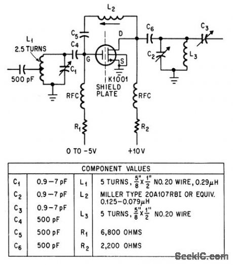
Capacitor C5 between dmin and gate provides neutralization by nullifying feedback. Neutrctlized stable gain at 250 Mc is 8 db. Bandwidth is 12 Mc.-P. E. Kolk and I. A. Maloff, The Field-Effect Transistor as High-Frequency Ampliler, Electronics, 37:31, p 71-74. (View)
View full Circuit Diagram | Comments | Reading(599)
BROADBAND_IMPEDANCE_TRANSFORMER
Published:2009/7/10 2:10:00 Author:May
Darlington circuit gives unity gain from d-c up to several Mc, using any complementary pair of transistors having sufncienlly high gain and cutoff frequency.-I. Ingemarsson, Darlington Maintains Constant Unity Gain, Electronics, 38:22, p 69.
(View)
View full Circuit Diagram | Comments | Reading(735)
45_34V_VARIABLE_AT_1A
Published:2009/7/19 22:45:00 Author:Jessie
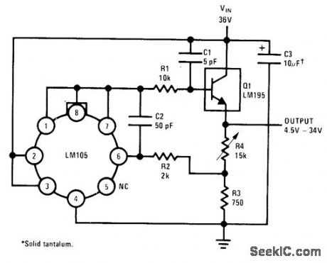
National LM195 power transistor is used with LM105 regulator to give fully adjustable range of output voltages with overload protection and only 2-V input-to-output voltage differential. Load regulation is better than 2 mV.-R. Dobkin, Fast IC Power Transistor with Thermal Protection, National Semiconductor, Santa Clara, CA, 1974, AN-110, p4. (View)
View full Circuit Diagram | Comments | Reading(715)
LIGHT_PROBE
Published:2009/7/10 2:10:00 Author:May
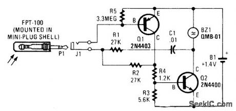
Originally designed as an aid for blind people, this probe was used as a light detector in order to tell if a device or room lights are on or off. (View)
View full Circuit Diagram | Comments | Reading(914)
TWO_STAGE_MOS_FET
Published:2009/7/10 2:09:00 Author:May
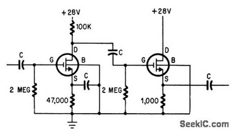
Pain of 3N98 transistors give voltage gain of 10 with low output impedance.-D. M. Griswold, Understanding and Using the MOS FET, Electronics, 37:31, p 66-70. (View)
View full Circuit Diagram | Comments | Reading(921)
SENSITIVE_SWR_METER
Published:2009/7/10 2:09:00 Author:May
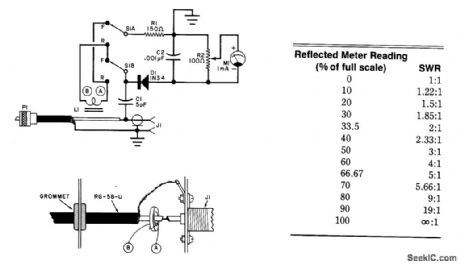
Using a toroidal pickup coil around the center conductor of a coaxial cable,this circuit can be used tomeasure the SWR of an antenna.L1 is two turns ﹟26 enameled wlre on a Fair-Rite 5963000301 toroidalcore. (View)
View full Circuit Diagram | Comments | Reading(3424)
| Pages:845/2234 At 20841842843844845846847848849850851852853854855856857858859860Under 20 |
Circuit Categories
power supply circuit
Amplifier Circuit
Basic Circuit
LED and Light Circuit
Sensor Circuit
Signal Processing
Electrical Equipment Circuit
Control Circuit
Remote Control Circuit
A/D-D/A Converter Circuit
Audio Circuit
Measuring and Test Circuit
Communication Circuit
Computer-Related Circuit
555 Circuit
Automotive Circuit
Repairing Circuit