
Circuit Diagram
Index 855
15_volt_LED_flasher_using_an_LM3909
Published:2009/7/19 23:41:00 Author:Jessie
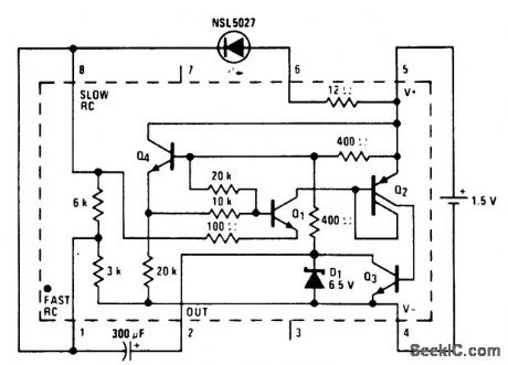
1.5-volt LED flasher using an LM3909. Flashing rate is about 1 hertz. Circuitry inside dashed lines is the LM3909 (courtesy National Semiconductor Corporation). (View)
View full Circuit Diagram | Comments | Reading(712)
VLF_AUDIO_TONE_GENERATOR
Published:2009/7/10 1:10:00 Author:May
Using an LC-tuned circuit, this oscillator can produce frequencies of less than 10Hz. C1 and C2 can be as large as 100μF. (View)
View full Circuit Diagram | Comments | Reading(643)
TEMPERATURE_STABLE_200_MC
Published:2009/7/19 23:40:00 Author:Jessie
Varies less than 2 Mc in frequency and less than 1.5 mw in power output over temperature range of 25 to 80℃. Normal power output is 22.5 mw. -Texas Instruments Inc., Solid-State Communications, McGraw-Hill, N.Y., 1966, p 301. (View)
View full Circuit Diagram | Comments | Reading(793)
MAKE_LM324_OP_AMP_SWING_RAIL_TO_RAIL
Published:2009/7/10 1:09:00 Author:May
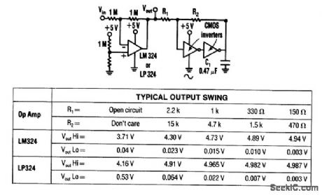
By using two CMOS inverters, the output for an LM324 op amp can be increased from 3.5 Vpp to 4.9 Vpp. This circuit is only recommended for light loads (<30 mA) and for relatively slow op amps. Any CM0S inverter (74C00, 74C02, 74C14, CD4001, CD4011, etc.) can be used. (View)
View full Circuit Diagram | Comments | Reading(1592)
3_volt_ministrobe_using_an_LM3909_chip
Published:2009/7/19 23:40:00 Author:Jessie
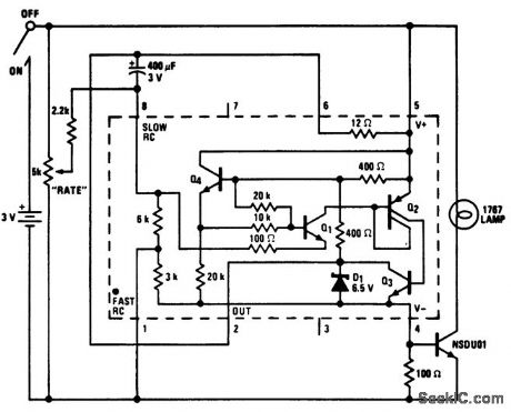
3-volt ministrobe using an LM3909 chip. Circuitry inside dashes is the LM3909. Flash rate can be varied from no flash to continuously on (courtesy National Semiconductor Corporation). (View)
View full Circuit Diagram | Comments | Reading(871)
TWO_TRANSISTOR_SINE_WAVE_OSCILLATOR
Published:2009/7/10 1:07:00 Author:May
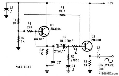
This oscillator uses two transistors and operates the crystal in the fundamental mode. C1 and C2 should be about 2 700 pF for 1 MHz, 680 pF for 5 MHz, and 330 pF for 10 MHz. 150 pF can be used for up to 20 MHz. The output is a near perfect sine wave. Try varying C1 and C2 for best waveform. About 2 to 6 Vpp is available. (View)
View full Circuit Diagram | Comments | Reading(2720)
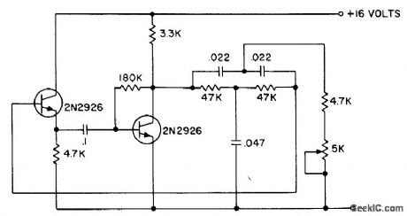
NONLINEAR_VOLTAGE_CONTROLLED_OSCILLATOR
Published:2009/7/19 23:39:00 Author:Jessie
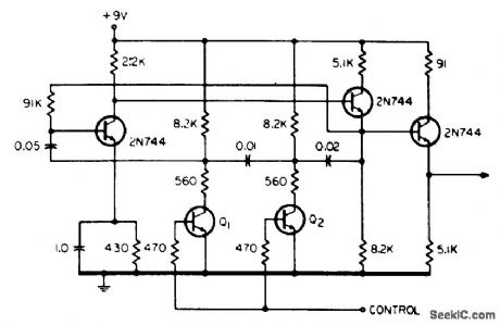
Use of conventional transistors rather than fet's means that Q1 and Q2 operate in knee region, where frequency does not vary linearly with d-c control voltage. This is generally not a drawback when control voltage is servoed. Increasing the control voltage increases the frequency.-R. Selleck, Voltage-Controlled Oscillators, EEE, 13:3, p 47. (View)
View full Circuit Diagram | Comments | Reading(803)
60_Hz_SINE_WAVE_GENERATOR
Published:2009/7/10 1:06:00 Author:May
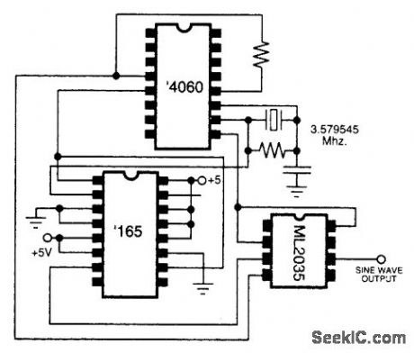
A chip by Micro Linear and two CMOS (40165 and 4060) chips generate sine waves at 60 Hz. (View)
View full Circuit Diagram | Comments | Reading(1800)
FOUR_TRANSISTOR_A_C_LINE_SET
Published:2009/7/19 23:39:00 Author:Jessie
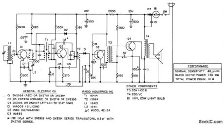
Nominal sensitivity is 40 microvolts per meter, power output 750 mw, and total power drain 10 w. - Transistor Manual, Seventh Edition, General Electric Co., 1964, p 297. (View)
View full Circuit Diagram | Comments | Reading(689)
PURE_SINE_WAVE_GENERATOR
Published:2009/7/10 1:04:00 Author:May

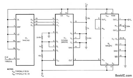
This circuit produces a pure, -80-dB THD sine wave with a frequency that is equal to thefc of IC3's filter. A TTL counter, an 8-channel analog multiplexer, and a fourth-order low-pass filter can generate 1- to 25-kHz sine waves with a THD of better than -80 dB. The circuit cascades the two second-order, contin-uous-time Sallen-Key filters within IC3 to implement the fourth-order low-pass filter. Two resistive dividers connected from ground to VDD and ground toVSS provide bipolar dc inputs to the multiplexer.To operate the circuit, you first must choose the filter's cutoff frequency, fc, by tying IC3's Do through D6 inputs to 5 V or ground. The cutoff frequency can be at 128 possible levels between 1 and 25 kHz, depending on those 7 digital input levels. Because this figure ties Do through D6 to ground, fc equals 1 kHz. The 100-kHz potentiometer adjusts the output level anywhere from 1.5 V below VDD to 1.5 V above VSS.The clock input frequency must be 8 times higher than the ftlter's fc. The multiplexer then produces an 8x oversampled staircase approximation of a sine wave. 8x oversampling greatly simplifies the smoothing requirements of the low-pass filter by pushing the first significant harmonic out to 7 x the funda-mental. All higher-order harmonics are removed by IC3, which includes an uncommitted amplifier for set-ting the output level. (View)
View full Circuit Diagram | Comments | Reading(3025)
BRIDGED_T_R_C_PHASE_SHIFT_OSCILLATOR
Published:2009/7/19 23:37:00 Author:Jessie
Emitter-follower eliminates loading variations, contributing to exceptional frequency stability (0.2%) over temperature range of -55 to 80℃.- Transistor Manual, Seventh Edition, General Electric Co., 1964, p 207. (View)
View full Circuit Diagram | Comments | Reading(751)
MULTIPLE_APERTURE_WINDOW_DISCRIMINATOR
Published:2009/7/10 0:59:00 Author:May
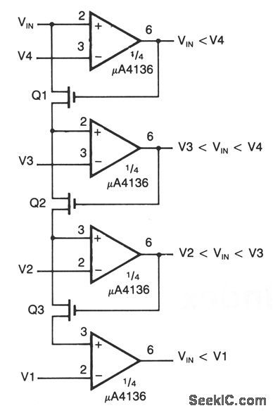
The circuit shown here uses μA4136 comparators and FETs Q1 through Q3. (View)
View full Circuit Diagram | Comments | Reading(2192)
SINE_WAIF_GENERATOR
Published:2009/7/10 0:59:00 Author:May
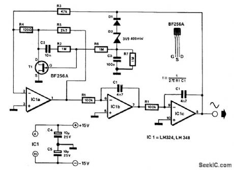
The frequency of the generator is determined by integrators IC1B and IC1C. An integrator has two properties that are used in this design. Firstly, a phase shift of 90° is between the input and output (ignor-ing, for the moment, the nonideal behavior of the op amp), and secondly, its amplification is - 1 (i.e., the signal inverts), provided the frequency:Cascading two identical integrators will thus result in an overall phase shift of 180° and an amplification of unity (provided that the frequency is1/2π/R1C1): an ideal basis for art oscillator. The two integrators are connected in the feedback circuit of an amplifier whose gain is determined by the amplitude of the output signal. Consequently, the generator has reasonably stable output voltage (at a level of about 4.5 Vpp).With the values of C1 (C1') and RI (R1'), as shown in the diagram, the output has a frequency of about 300 Hz. The frequency can be varied by replacing R1and R1' with a stereo potentiometer. To keep the frequency setting within bounds, the overall range of this potentiometer should not exceed a decade.The maximum attainable frequency is about 5 kHz. Distortion is not greater than 0.10/0. The current drawn by the generator is only a few milliamperes. Finally, the LM348 is a quadruple 741; it is thus possi-ble to construct the generator from four 741s. (View)
View full Circuit Diagram | Comments | Reading(1534)
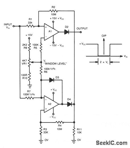
SIMPLE_WINDOW_DETECTOR
Published:2009/7/10 0:57:00 Author:May
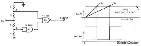
This simple window detector uses only half of a 7400 quad NAND gate plus four resistors, chosen so that the voltage at point A exceeds the voltage at point B for any input voltage. With no input applied or when VIN is at ground, the output of gate G1 is one; hence G2's output is also one. As the input voltage increases, VA, rises faster than VB. When VA reaches an acceptable one level, the circuit's output drops to zero. As the input continues to increase, VB rises to an acceptable level, changing the output of G2 to one. (View)
View full Circuit Diagram | Comments | Reading(857)
COMPOUND_OP_AMP_VCO_DRIVER
Published:2009/7/10 0:57:00 Author:May
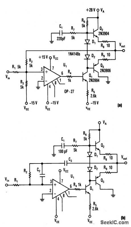
This circuit produces 5-to 25-V output to drive a VCO from a standard ±15-V supply system. R7 and C1 supply frequency compensation. Q1 through Q3 form an inverting amplifier with a gain of two.Negative feedback through R2 closes the loop. This circuit can act as a an active load-log filter and directly drive a voltage-controlled oscillator. (View)
View full Circuit Diagram | Comments | Reading(903)
SAMPLE_AND_HOLD
Published:2009/7/10 0:56:00 Author:May
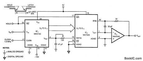
By using the ADO and DAC, this circuit uses a negative pulse to latch data into the ADO. The hold pulse width should be at least 8.5 μs. This circuit has zero drop and infinite hold time. (View)
View full Circuit Diagram | Comments | Reading(0)
RF_UPCONVERTER_FOR_TVRO_SUBCARRIER_RECEPTION
Published:2009/7/10 0:54:00 Author:May
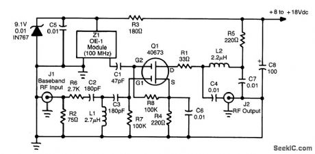
This converter uses a 40673 MOSFET to heterodyne the 5.5- to 8-MHz TVRO subcarriers to the FM broadcast band, where a stereo receiver can be used for high-fidelity stereo reception of TV sound subcarriers. 21 is a prepackaged 100-MHz oscillator module, which is available from International Crystal Corporation, Oklahoma City, Ok. (View)
View full Circuit Diagram | Comments | Reading(690)
WINDOW_DETECTOR_3
Published:2009/7/10 0:54:00 Author:May
This novel window detector uses only two op amps。The width of the window can be changed by the 4.7-KΩ potentiometer. (View)
View full Circuit Diagram | Comments | Reading(725)
SIGNAL_POWERED_RECEIVER
Published:2009/7/19 23:36:00 Author:Jessie
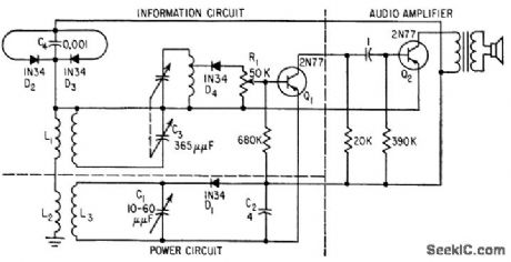
Circuit receives and reclines r-f radiation, stores resultant d-c energy in C2, and releases energy to transistors as required. Unique dipole rectifier provides efficient antenna-to-receiver coupling for frequencies of above 50 Mc.-L. It. Crump, Radio Waves Power Transistor Circuits, Electronics, 31:19, p 63-65. (View)
View full Circuit Diagram | Comments | Reading(693)
220_MHz_RECEIVING_CONVERTER
Published:2009/7/10 0:53:00 Author:May
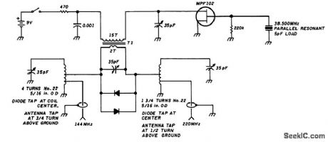
A simple circuit using a single transistor converts 220 MHz to 144 MHz or vice versa, because the mixer is bilateral. T1 has 15 turns on the primary, and 2 turns on the secondary (#24 AWG wire) on a 0.375 ID SF-material toroidal coil. (View)
View full Circuit Diagram | Comments | Reading(1623)
| Pages:855/2234 At 20841842843844845846847848849850851852853854855856857858859860Under 20 |
Circuit Categories
power supply circuit
Amplifier Circuit
Basic Circuit
LED and Light Circuit
Sensor Circuit
Signal Processing
Electrical Equipment Circuit
Control Circuit
Remote Control Circuit
A/D-D/A Converter Circuit
Audio Circuit
Measuring and Test Circuit
Communication Circuit
Computer-Related Circuit
555 Circuit
Automotive Circuit
Repairing Circuit