
Circuit Diagram
Index 847
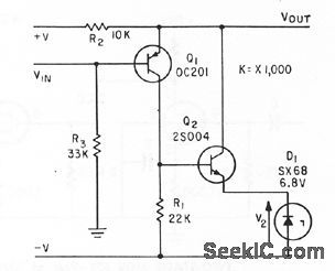
_3_V_BATTERY_TO__5_Vdc_dc_CONVERTER
Published:2009/7/10 2:04:00 Author:May
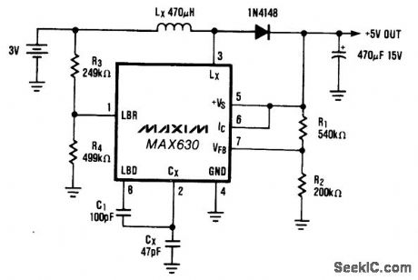
A common power-supply requirement involves converting a 2.4- or 3-V battery voltage to a 5-V logic supply. This circuit converts 3 V to 5 V at 40 mA with 85% efflciency. When IC (pin 6) is driven low, the output voltage will be the battery voltage minus the drop across diode D1. The optional circuitry that uses C1, R3, and R4 lowers the oscillator frequency when the battery voltage falls to 2.0 V. This lower frequency maintains the output-power capability of the circuit by increasing the peak inductor current, which compensates for the reduced battery voltage. (View)
View full Circuit Diagram | Comments | Reading(703)
9_TO_5_V_CONVERTER
Published:2009/7/10 2:02:00 Author:May
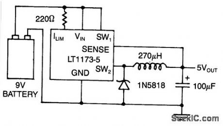
Using a Linear Technology LT1173-5, this converter produces regulated 5 V from a 9-V battery. (View)
View full Circuit Diagram | Comments | Reading(685)
30_MC_LINEAR_SSB
Published:2009/7/10 2:02:00 Author:May
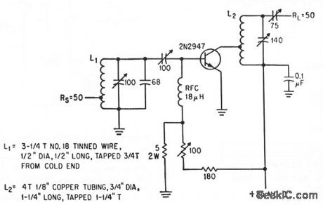
Power gain is 13 db and output is 8 w peak envelope power.-L. E.Clark, E. B. Mack, and R. C. Heihall, Highlights of Small-Signcd Circuit Design, Electronics, 36:49, p 46-50. (View)
View full Circuit Diagram | Comments | Reading(635)
Bipolar_voltage_to_frequency_converter
Published:2009/7/19 22:36:00 Author:Jessie
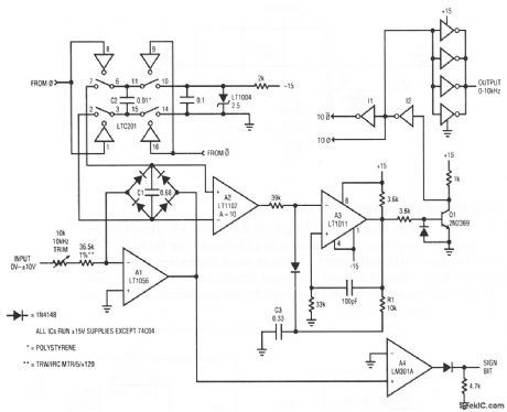
This circuit produces a 0- to 10-kHz output in response to a 0- to ± 10-V input. The A4 output indicates the sign (+ or -) of the input. To calibrate, apply either a - 10- or + 10-V input and set the 10-kΩ trim for exactly a 10-kHz output. The low offsets of A1 and A2 permit operation down to a few Hz with no zero trim required. Linear Technology Corporation 1991 AN45-17 (View)
View full Circuit Diagram | Comments | Reading(703)
COMPOUNDED_EMITTER_FOLLOWER
Published:2009/7/10 2:01:00 Author:May
Compounded emitter-follower with feedback, operctted as complementary pair, gives higher input impedance, higher gain, and lower output impedance than conventionol eminerfollower.-T. K. Hemingway and J. Willis, Transistor Pairs Improve Emitter-Follower Performance, Electronics, 35:21, p 48-49. (View)
View full Circuit Diagram | Comments | Reading(770)
1_TO_5V_dc_dc_CONVERTER
Published:2009/7/10 2:01:00 Author:May
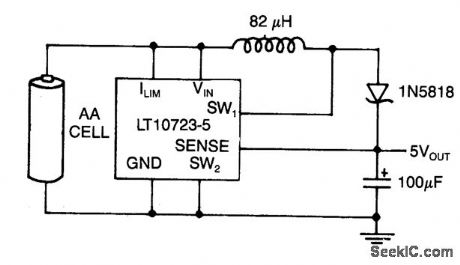
This circuit, using the Linear Technology LT1173,produces 5 V at 40 mA from a 1.5-V AA cell. (View)
View full Circuit Diagram | Comments | Reading(1535)
DOUBLECONVERSION_F_M_SUPERHETERO_DYNE
Published:2009/7/19 23:26:00 Author:Jessie
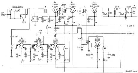
Common-base connections in local oscillators Q10 and Q11 give stability with minimum components in 20.channel Mercury spacecraft command receiver. Each frequency multiplier doubles frequency of first local oscillator. If output is 10.7 Mc.-R. Elliott, First Details on Mercury Spacecraft Command Receiver, Electronics, 36:5, p 32-35.
(View)
View full Circuit Diagram | Comments | Reading(1428)
NR_DIODE_AS_R_F_OSCILLATOR
Published:2009/7/19 23:25:00 Author:Jessie
Simple negative-resistance diode circuit can develop several milliwatts at frequencies up to 300 Mc.-A. P. Schmid, Jr., Negative-Resistance Diode Handles High Power, Electronics, 34:34, p 44-46. (View)
View full Circuit Diagram | Comments | Reading(677)
OPTICAL_LASER_RECEIVER
Published:2009/7/10 2:01:00 Author:May
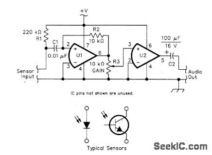
Using a single 741 op amp, a photodiode sensor, and an LM386, this simple receiver operates from a 9-V battery. The circuit will drive a pair of earphones or a small speaker. (View)
View full Circuit Diagram | Comments | Reading(2124)
CB_CRYSTAL_OSCILLATOR
Published:2009/7/19 23:24:00 Author:Jessie
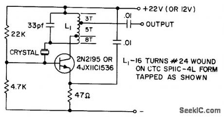
Uses low-cost crystal having high series resistance, up to 30 ohms. Provides adequate output to supply most master oscillator-power amplifier applications. Output tap is arranged to match directly a companion 2N2195 grounded-base amplifier. Crystal is 3rd overtone type.- Transistor Manual, Seventh Edition, General Electric Co., 1964, p 211. (View)
View full Circuit Diagram | Comments | Reading(953)
MILLIMETER_WAVE_DETECTOR
Published:2009/7/19 23:24:00 Author:Jessie
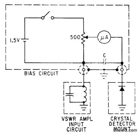
Biasing with 1N53 crystal detector increases gain 20 db at 73 Mc.-K. Ishii and A. L. Brault, Crystal Biasing Improves Millimeter-Wave Detector, Electronics, 34:24, p 65. (View)
View full Circuit Diagram | Comments | Reading(804)
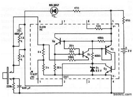
ELECTRONIC_SIREN
Published:2009/7/10 2:01:00 Author:May
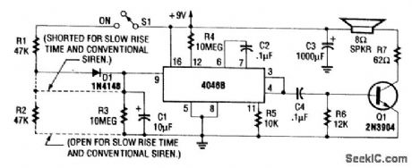
For normal wailing tone, short D1 and open R2. For fast rise and slow fall in frequency, include D1 and R2. Use of a CD4046B with a diode-RC network as shown produces a siren tone, using a VCO. (View)
View full Circuit Diagram | Comments | Reading(0)
CARRIER_CURRENT_TRANSMITTER
Published:2009/7/19 23:23:00 Author:Jessie
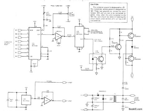
Modulates existing house wiring with high-frequency signals that can bedetected by special receivers plugged into any AC outlet, for control of appliances by home computer. Applications include turning house lights on and off during owner's absence on elaborate time schedule programmed into computer. IC1 converts 8-bit data word from computer to proportional analog output current. This is converted to voltage by IC2 for control of VCO IC3 that gives frequency proportional to voltage. With values shown, range is about 30 to 110 kHz, with 256 discrete increments of frequency. Thus, input code 00000000 gives 30 kHz, 00000001 gives 30.3 kHz, and 01000000 (decimal 64} gives 49.2 kHz. Signal is applied to house wiring by 0.5-W power amplifier Q1-Q3, using optical coupling through IC4 to prevent computer circuit from interacting with house wiring. Supply voltage ±V is 11 to 13 V. T1 is 12.6-VAC 300-mA filament transformer. ICS is 2 to 2.5 V reference chip such as MC1403U. System uses one frequency to turn receiver on and frequency 4 kHz above or below in 8-kHz band to turn it off, for maximum of ten control channels in system. Article covers calibration of transmitter.-S. Ciarcia, Tune in and Turn on, Part 1:A Computerized Wireless AC Control System, BYTE, April 1978, p 114-116, 118, 120, and 122-125 (Part 2-May 1978, p97-100 and 102).
(View)
View full Circuit Diagram | Comments | Reading(0)
Indicating_one_shot
Published:2009/7/19 23:23:00 Author:Jessie
In this application, the LM3909 delivers an approximate 1/2-s flash from the LED every time that the pushbutton makes contact (momentary or held).Such circuits are used with keyboards, limit switches, and other mechanical contacts that must feed data into electronic digital systems. National Semiconductor, Linear Applications Handbook 1991 p 406 (View)
View full Circuit Diagram | Comments | Reading(795)
CASCODE_MOS_FET
Published:2009/7/10 2:00:00 Author:May
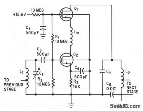
Power gain is slightly higher than for neutralized commonsource stage.-G. G. Luettgenau and S. H. Barnes,Designing Wilh Low-Noise MOS FETs:A Little Different But No Harder, Electronics,37:31,p 53-58. (View)
View full Circuit Diagram | Comments | Reading(839)
AC_SOLID_STATE_RELAYS
Published:2009/7/10 2:00:00 Author:May
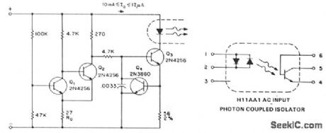
In the case where analog signals are being used as the logic control, hysteresis from a Schmitt-trigger input can be used to prevent half-wave power output. The circuit operation is as follows: at low input voltages, Q1 is biased in the off state. Q2 conducts and biases Q3, and the IRED turns off. When the base of Q1 reaches the biasing voltage of 0.6 V, plus the drop across RD, Q1 turns on. Q3 is then supplied base drive, and the solid-state relay input will be activated. The combination of Q3 and Q4 acts as a constant-current source to the IRED. In order to turn-off Q3, the base drive must be reduced to pull it out of saturation. Because Q2 is in the off-state as the signal is reduced, Q1 will now stay on to a base bias-voltage lowered by the change in the drop across RD. With these values, the highest turn-off voltage is 1.0 V, while turn-on will be at less than the 4.1 V supplied to the circuit.For ac or bipolar input signals, there are several possible connections. If only positive signals are set to activate the relay, a diode, such as the A14, can be connected in parallel to protect the IRED from reverse voltage damage, since its specified peak reverse voltage capability is approximately 3 V. If ac signals are being used, or if activation is to be polarity insensitive, a H11AA coupler, which contains two LEDs in antiparallel connection, can be used. For high-input voltage designs, or for any easy means of converting a dc input relay to ac, a full-wave diode bridge can be used to bias the IRED. (View)
View full Circuit Diagram | Comments | Reading(965)
_TWO_TRANSISTOR_REFLEX_RADIO
Published:2009/7/19 23:23:00 Author:Jessie
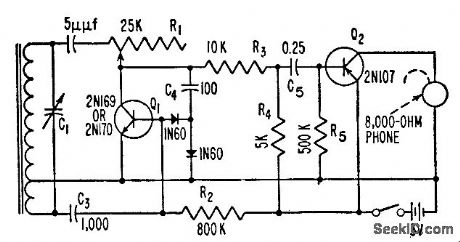
Q1 is used regeneratively as r-f amplifier and reflexively as first a-f amplifier, while Q2 serves as power amplifier.-S. A. Sullivan, Transistor Radio Uses Few Parts, Electronics, 31:1, p 90-92. (View)
View full Circuit Diagram | Comments | Reading(1599)
CONSTANT_GAIN
Published:2009/7/10 1:59:00 Author:May
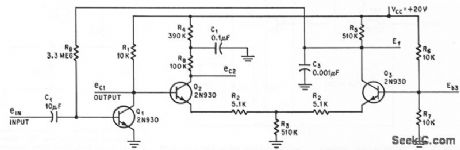
Differentical amplifier Q2-Q3 regulates bias of Q1 to keep gain constanl despite voriations in load or In circuit componenls.-R,C, lavigne and L.L. Kleinberg, Amplifier Gain is Constant Despite Changes in Load, Electronics, 38:13, p 75-77. (View)
View full Circuit Diagram | Comments | Reading(668)
Low_voltage_lamp_flasher_using_a_PUT_and_two_SCRs
Published:2009/7/19 23:23:00 Author:Jessie
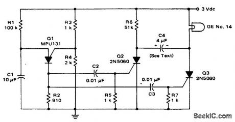
Low-voltage lamp flasher using a PUT and two SCRs. C4 is a nonpolarized type capacitor (courtesy Motorola Semiconductor Products Inc.). (View)
View full Circuit Diagram | Comments | Reading(740)
FOUR_TRACE_OSCILLOSCOPE_ADAPTER
Published:2009/7/10 1:59:00 Author:May
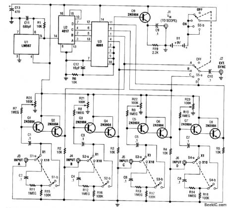
This simple adapter uses an oscillator (567) to drive a counter (U2) and switch (U3) that selects the output of one of four scope preamps (Q1/Q2 through Q7/Q8) and feeds it to buffer Q9 and output jack J1. J2 provides synch to the scope. R20 through R23 are posting controls for channels A through D (J3 through J6). SlA-B through S4A-B are switched attenuators, one for each channel. Switching rate is about 125 kHz. This circuit is useful for adding four-trace operation to inexpensive oscilloscopes. Signal levels of 0 to 20 V can be handled. (View)
View full Circuit Diagram | Comments | Reading(941)
| Pages:847/2234 At 20841842843844845846847848849850851852853854855856857858859860Under 20 |
Circuit Categories
power supply circuit
Amplifier Circuit
Basic Circuit
LED and Light Circuit
Sensor Circuit
Signal Processing
Electrical Equipment Circuit
Control Circuit
Remote Control Circuit
A/D-D/A Converter Circuit
Audio Circuit
Measuring and Test Circuit
Communication Circuit
Computer-Related Circuit
555 Circuit
Automotive Circuit
Repairing Circuit