
Circuit Diagram
Index 850
Stereo_record_player_AF_preamplifier_with_bass_and_treble_controls_for_magnetic_pickup
Published:2009/7/20 1:37:00 Author:Jessie
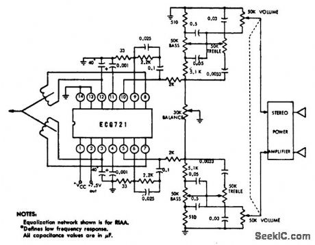
Stereo record player AF preamplifier, with bass and treble controls, for magnetic pickup. Current drain is typically 16 mA at 12 volts. Voltage gain is 68 dB. Channel separation is typically 60 dB (courtesy GTE Sylvania Incorporated). (View)
View full Circuit Diagram | Comments | Reading(1046)
STABILIZED_DIRECT_COUPLED_A_C_AMPLIFIER
Published:2009/7/10 1:47:00 Author:May
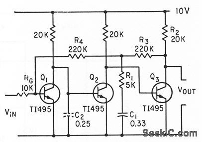
Current-derived stabilization gives simple ampliler using only one capacitor. Adding C2 improves stability but lowers cutoff frequency.-P. Laakmann, Direct Coupling Shrinks Amplifer Size and Cost, Electronics, 36:12, p 66-48. (View)
View full Circuit Diagram | Comments | Reading(803)
SUPER_SOUND_GENERATOR
Published:2009/7/10 1:47:00 Author:May
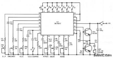
Six preset controls and seven selector switches enable a vast range of different sounds to be produced and altered at will. Such sounds as steam trains chuffing, helicopters flying, bird chirping, and machine guns firing are possible, as well as the usual police sirens, phaser suns, and bomb explosions. The circuit incorporates an amplifier giving 150-mW output into a small loudspeaker. Alternatively, a separate amplifier system can be used for disco effects, car alarms, etc. Continuous or one-shot sounds are possible. For one-shot sounds, a push-button switch is prodded, which can also be used to turn continuous sounds on and off. A single IC, SN76477, provides all of the sound generation circuits. (View)
View full Circuit Diagram | Comments | Reading(1960)
UNITY_GAIN_BUFFER
Published:2009/7/10 1:47:00 Author:May
Positive gain of unity is obtained with high input impedance, low output impedance, negligible phase shift, and without phase reversal. Can be used for isolating resolvers from loads.-D. K. Phillips, Unity-Gain Buffer Acquires Precision by Feed-back, Electronics, 36:51, p 36-37. (View)
View full Circuit Diagram | Comments | Reading(0)
LINEAR_IC_SIREN
Published:2009/7/10 1:45:00 Author:May


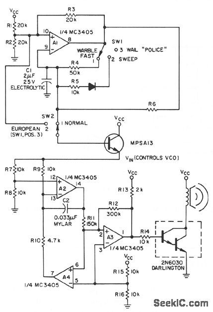
A low-frequency, op-amp oscillator and a VCO, both configured from a single MC3405 dual op amp and dual comparator, are the major components in a siren circuit that can be made to produce various warbles and wails, or serve as an audio sweep generator. The only other active components needed are an MPS A13 small-signal transistor and a 2N6030 power Darlington transistor. (View)
View full Circuit Diagram | Comments | Reading(744)
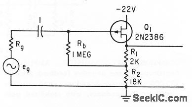
NEUTRALIZED_MOS_FET
Published:2009/7/10 1:45:00 Author:May
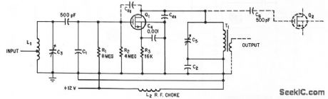
Delivers power gain of 20 db at 100 Mc, with common-source connection.-G.C.Luettgenau and S.H.Barnes,Designing With Low-Noise MOS FETs:A Little Different But No Harder,Electronics,37:31,p 53-58. (View)
View full Circuit Diagram | Comments | Reading(671)
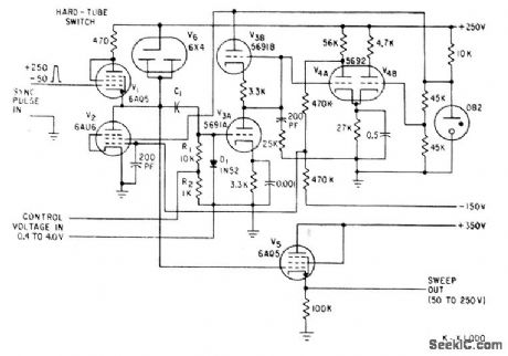
RECTANGULAR_TRIANGULAR_WAVEFORM_CONVERTER
Published:2009/7/10 1:44:00 Author:May
Many function generators are based on a rectangular waveform generator that consists or a Schmitt trigger and integrator. The triangular signal produced by the integrator is then used to form a sinusoidal signal with the aid of a diode network. The converter presented here works the other way around. It con-verts the output of a good-quality sine-wave oscillator into a rectangular and a triangular siant.
The sinusoidal siinal is converted into a rectangular signal by IC2A. Because the output of this gate varies between - 15 V and + 15 V, it is reduced to a value that is suitable for integration by potential divider R3/R4. It is then integrated by transconductance amplifier IC1A and C2. The amplifier has a current output that is controlled by the current through pin 1. The output therefore behaves as a resistance, with which it is possible to influence the integration time.
The voltage across C2 is available in buffered form at the output of impedance inverter IC2B; this is the triangular signal. The amplitude of this signal is compared with a voltage set by P2 and the difference between these voltages, which is the output of IC2C, is applied to the current source at the output of IC1 via R5. This arrangement ensures that the level of the output voltage is virtually independent of the frequency of the rectangular signal or of the sinusoidal input.
One problem with a precision integration is its being affected by offset voltages and bias currents. Feedback loop R6/C1 ensures that the output follows the potential across R4 accurately. However, tiny deviations might be caused by the bias current in circuit IC1, which is not greater than 8 μA at 70℃.The time constant R6/C1 is large for a purpose: to ensure that the triangular signal, even at low fre-quencies, cannot affect the waveform of the signal to be integrated-the rectangular shape must be retained. The converter can process signals at frequencies from 6 Hz (where the amplitude is not affected) to 60 kHz (where the amplitude is reached by 10%).
Because of the long time constants, the time taken for the recovery of the amplitude of the triangular signal at frequencies above 1 kHz is rather long. The peak value of this signal should be set to 1 V.
Diode D1 is a so-called sfaGa'slot-three diodes in one package. It might be replaced by three discrete type 1N4148 diodes. The current drawn by the converter is of the order of 9 mA.
(View)
View full Circuit Diagram | Comments | Reading(1649)
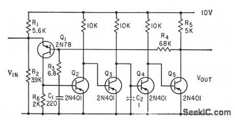
TIMED_TONE_DECODER
Published:2009/7/20 1:37:00 Author:Jessie
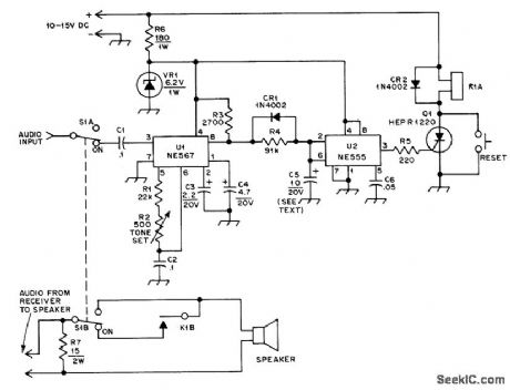
Uses NE567 PLL and 555 timer to activate muted monitoring receiver until alerting audio tone of correct frequency and duration is received. Can be applied to almost any receiver for weather emergency alert warnings, paging calls, and similar services without having to listen continously to other traffic on channel, if received tone is within bandwidth of tone decoder, output of U1 goes nearly to zero and C5 starts to discharge through R4. When voltage at pins 2 and 6 of U2 reaches one-third of supply voltage, output of U2 goes high and triggers SCRQ1, energizing 12-V relay K1. Values shown for C4 and C5 give 1-s delay, which means triggering tone must be on at least 1 s. Once SCR is triggered, it holds relay on even after tone ceases. Pushbutton switch shorts SCR and releases relay when reset is desired. Zener provides regulated 6.2 V required for decoder. Values shown for R1, R2, and C2 give response to 450-Hz tone. Avoid use of Touch-Tone frequency, to prevent accidental triggering by those using Touch-Tone system.-J. S. Paquette, A Time-Delayed Tone Decoder, QST; Feb. 1977, p 16-17. (View)
View full Circuit Diagram | Comments | Reading(930)
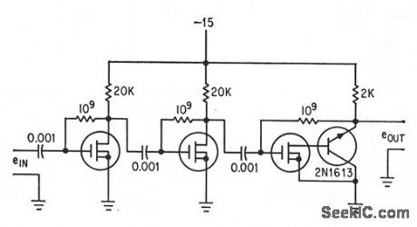
SOURCE_FOLLOWER_USES_BOOTSTRAPPING
Published:2009/7/10 1:44:00 Author:May
Bandwidth is 10 cps to 10 kc, d-c input impedance is 10 meg, and input impedance at 10 kc is above 1 meg for input signals from 1 my to 10 my.-T. R. Bignell, How to Get Maximum Input Impedance with Field-Effect Transistors, Electronics, 36;10, p 44-46. (View)
View full Circuit Diagram | Comments | Reading(760)
FACSIMILE_SWEEP
Published:2009/7/20 1:36:00 Author:Jessie
Maximum variation in sweep length is less than 1 part in 1,000. Uses modified Miller feedback circuit. Sweep role can be controlled over 10:1 ratio.-E. W. Van Winkle, High-Precision Sweep Generator, Electronics, 33:50, p 88-90. (View)
View full Circuit Diagram | Comments | Reading(1076)
THE_WAILING_SIREN
Published:2009/7/10 1:44:00 Author:May
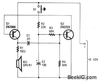
Transistors Q1 and Q2, with feedback provided via C1 from the collector of Q1 to the base of Q2, forms a voltage-controlled oscillator (VCO). Depending on the voltage applied to Q2's base, the VCO frequency ranges from around 60 Hz to 7.5 kHz. The instantaneous voltage applied to the base of Q2 is determined by the values of C2, R2, R3, and R4. When pushbutton switch S1 is closed, C2 charges fairly rapidly to the maximum supply voltage through R2, a 22-KΩ fixed resistor. That causes the siren sound to rise rapidly to its highest frequency. When the button is released, the capacitor discharges through R3 and R4 with a combined resistance of 124 KΩ, causing the siren sound to decay from a high-pitched wail to a low growl. If you want to experiment with the pitch of the sound at its highest frequency, try different values for C1. ncrease its value for lower notes, and decrease it for higher ones. Different values for R2 will change the attack time. A 100-KΩ resistor provides equal attack and decay times. The way you handle the pushbutton varies the effect. (View)
View full Circuit Diagram | Comments | Reading(1101)
BROADBAND_WITH_GAIN_OF_1350
Published:2009/7/10 1:43:00 Author:May
Metal oxide semkonductor transistors (p-mosts) in Darlington contguration give high input impedance and low output impedance from 5 cps to 72 kc.-F. M. Wanklss, Novel Field-Effect Devke Provides Broadband Gain, Electronics, 36A4, p 30-33. (View)
View full Circuit Diagram | Comments | Reading(804)
1_watt_power_amplifier
Published:2009/7/20 1:36:00 Author:Jessie
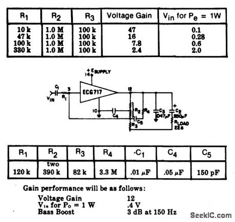
1-watt power amplifier. Refer to the table to select the desired voltage gain. In the circuit the AC feedback path is different from the DC path. Resistor R2 is bypassed to ground, taking it out of the AC feedback loop. The voltage gain is determined by the ratio of R4/R1. Another feature of this circuit is that you can introduce bass boost by the selection of capacitor values for C1, C4 and C5. With the values shown in the table at the bottom of the figure, gain performance is as follows: voltage gain is 12, VIN for Po at 1W is 0.4 volt, and bass boost is 3 dB at 150 Hz (courtesy GTE Sylvania Incorporated). (View)
View full Circuit Diagram | Comments | Reading(788)
General_purpose_fixed_gain_low_distortion_amplifier_using_an_ECG716_that_can_be_employed_for_such_things_as_a_telephone_or_headset_AF_amplifier
Published:2009/7/20 1:34:00 Author:Jessie
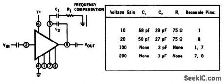
General-purpose fixed-gain low-distortion amplifier, using an ECG716, that can be employed for such things as a telephone or headset AF amplifier. Fixed voltage gain of 10, 20, 100, and 200 can be obtained by referring to the table. Supply voltage is 27 volts, input voltage is ±5 volts, and power dissipation is 600 mW. Voltage gain falls off sharply above 1 MHz (courtesy GTE Sylvania Incorporated). (View)
View full Circuit Diagram | Comments | Reading(641)
SOURCE_FOLLOWER_WITH_REDUCED_GATE_TO_DRAIN_CAPACITANCE
Published:2009/7/10 1:42:00 Author:May
Diode D1 gives maximum a-c bootstrapping of gate bias resistance while providing required d.c bias. Emitter-follower Q2 couples to drain of let al a signal in phase with input, to give extremely low input capacitance.-T. R. Bignall, How to Get Maximum Input Impedance with Field-Effect Transistors, Electronics, 36:10, p 44-46. (View)
View full Circuit Diagram | Comments | Reading(798)
PROGRAMMABLE_FREQUENCY_ADJUSTABLE_RATE_SIREN
Published:2009/7/10 1:42:00 Author:May
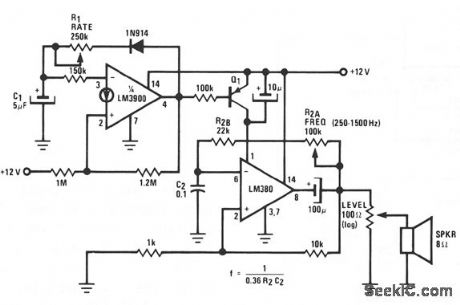
The LM380 operates as an astable oscillator with the frequency determined by R2/C2. Adding Q1 and driving its base, with the output of an LM3900 wired as a second astable oscillator, acts to gate the output of the LM380 on and off, at a rate fixed by R1/C1. (View)
View full Circuit Diagram | Comments | Reading(953)
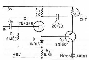
CURRENT_DERIVED__STABILIZATION
Published:2009/7/10 1:41:00 Author:May
Bridge-derived stabilization In direct-coupled a-c amplifier Provdes current sensitivity of 0.1 microamp per ma of output current.-P.Laakmann, Direct Coupling Shrinks Ampliler Size and Cost, Electronics, 36:12, p 66-68. (View)
View full Circuit Diagram | Comments | Reading(658)
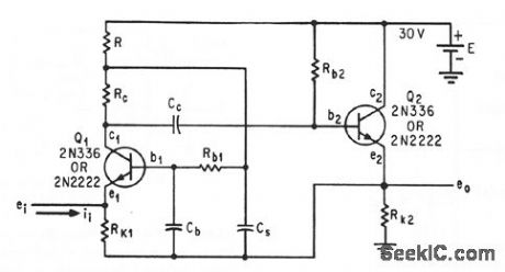
TRANSDUCER_EXCITER
Published:2009/7/20 1:34:00 Author:Jessie
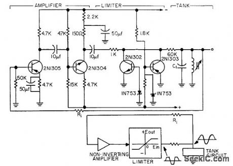
Used in carrier amp lifer of strip-chart recorder to provide amp litude-stable fixed excitation frequency for transducer. Two-stage amplifier with 360° phase shift oscillates when output is fed to input, al frequency depending on loop parameters. Amplitude variation is held to 0.2% for 25℃ change in ambient by simple zener and transistor limiter.-Amplitude-Stable Audio Oscillator, EEE, 11:8, p 87. (View)
View full Circuit Diagram | Comments | Reading(1445)
YELPING_SIREN
Published:2009/7/10 1:41:00 Author:May
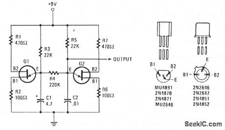
Unijunction transistors Q1 and Q2 are both connected as relaxation-type, sawtooth oscillators. Transistor Q1 is the low-frequency control oscillator and Q2 is the tone generator. Sawtooth waveforms are produced at the emitter terminals. Without R4 connecting the two emitters, each oscillator operates inde-pendently, with its frequency determined mainly by the re time constant. With the values shown, Q1 operates from 1. to 1.5 Hz and Q2 operates from 400 to 500 Hz. When R4 is connected between the two emitters, it couples the low-frequency sawtooth from Q1 directly across capacitor C2. That coupling causes the frequency of the tone generator to increase, along with the rise in sawtooth voltage from Q1.The tone generator's frequency drops to its lower design value when C1 discharges and produces the fall-ing edge of the sawtooth. (View)
View full Circuit Diagram | Comments | Reading(2351)
CARRIER_CURRENT_RECEIVER
Published:2009/7/20 1:33:00 Author:Jessie
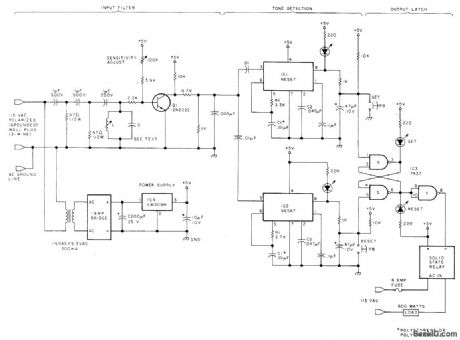
When it is plugged into AC line, receiver responds to pair of control frequencies 4 kHz apart in range of 30 to 110 kHz, placed on house wiring by computer-controlled transmitter, Receiver turns controlled device on or off through solid-state relay for which article gives suitable circuit, Tuned bandpass filter amplifies only that pair of frequencies assigned to its receiver, attenuating all other frequency pairs used in system.Amplified signal is sent to tone decoders IC1 and IC2, one responding to each frequency.Input filter provides attenuation of 60-Hz line frequency and all other frequencies except 8-kHz band of specific channel. LC bandpass circuit, set for center of desired passband, acts as passive filter. L is low-Q slug-tuned 1-10 mH coil, set at 2 mH when C is made 0.01μF for center frequency of 35 kHz. Article covers operation in detail and gives procedure for determining values of R1, C1, and 02 for each detector. Solid-state output relay can be Sigma 226 RE1-5A1, rated 6 A.-S. Ciarcia, Tune in and Turn on, Part 2:An AC Wireless Remote Control System, BYTE. May 1978,p97-100 and 102(Part 1- April 1978,p114-116,118,120,and 122-125). (View)
View full Circuit Diagram | Comments | Reading(0)
| Pages:850/2234 At 20841842843844845846847848849850851852853854855856857858859860Under 20 |
Circuit Categories
power supply circuit
Amplifier Circuit
Basic Circuit
LED and Light Circuit
Sensor Circuit
Signal Processing
Electrical Equipment Circuit
Control Circuit
Remote Control Circuit
A/D-D/A Converter Circuit
Audio Circuit
Measuring and Test Circuit
Communication Circuit
Computer-Related Circuit
555 Circuit
Automotive Circuit
Repairing Circuit