
Index 199
TV Signal Transformation Amplifier Circuit
Published:2011/5/18 9:41:00 Author:Joyce | Keyword: TV Signal, Transformation, Amplifier
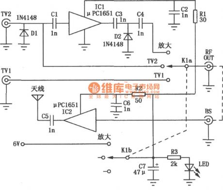
As shown in the figure is a circuit used to transform and amplify all kinds of TV video signals output by various equipment,such as VCR, DVD players with weak output signals to be amplified.It can send the open circuit with radio-frequency signals to an extent with 7m-radius to make it possible for several TV to function at the same time. (View)
View full Circuit Diagram | Comments | Reading(751)
Video Enhancement Circuit
Published:2011/6/6 0:23:00 Author:Joyce | Keyword: Video, Enhancement
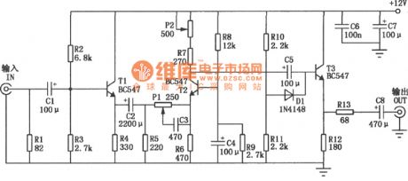
The video enhancement circuit shown in the graph can increase the high frequency component of video signals,thus enhancing the contrast of the televison image. It can be connected between the output end of VCR and the input end of television SCART. The transistorT1 in the circuit acts as a buffer. Resistance Rl guarantees that the input impedance of this circuit is about 75 Ω. Signals will be applied to the enlarger T2,and their gains depend on the position of the potentiometer P2. The frequency characteristics of T2 base signals are restricted by P1, R6, C6 ,so in a certain extent it can be controlled by the users (through P1). Buffer stage T3 provides enough electricity to drive most 75 Ω loads correctly .Adjusting potentiometer P2 can set the output to be 1Vp - p (electric level should be 2Vp - p for output to open circuit). (View)
View full Circuit Diagram | Comments | Reading(735)
Simulation Karaoke Accompaniment Amplifier Circuit
Published:2011/6/6 0:24:00 Author:Joyce | Keyword: Simulation , Karaoke Accompaniment , Amplifier
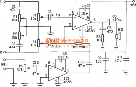
As shown in the figure is the simulation karaoke accompaniment amplifier circuit. According to the features of audiotapes, this circuit can remove the same part in the left and right channel of the stereo and leave the accompanying music . (View)
View full Circuit Diagram | Comments | Reading(3391)
put 4 ~ 20MA into the positive and negative 10 V current-voltage conversion circuit
Published:2011/5/11 21:53:00 Author:Fiona | Keyword: current-voltage conversion
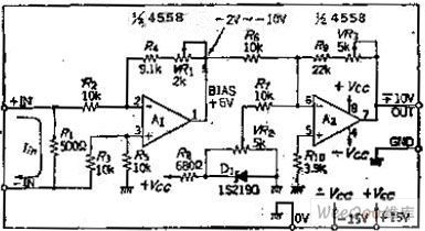
Circuit Work
The purpose of using OP amplifier A1 is to consider that if the one end of sensor resistance R1 can not be grounded, R1 can be used as a differential amplifier. However, if the resistance R6 and R7 of the summation meter have high value,you can remove A1. In order to make A3 output -10V when the current is 4MA, the A1 should be made output in -2 ~-10V.
OP amplifier A2 is the summing amplifier putting unipolar input into bipolar output. In order to output 0 when the current is 12MA, add the polar opposite +6 V for subtraction. VR3 is used to determine the slope. Because it should enlarge 8V which is input to 20V, so the magnification should be A = 20 / 8 = 2.5 times. (View)
View full Circuit Diagram | Comments | Reading(2482)
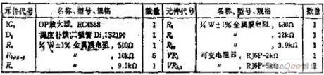
The thermocouple temperature/frequency converter circuit (02)
Published:2011/6/10 3:45:00 Author:Seven | Keyword: thermocouple, temperature/frequency converter
Notes: *IRC/TRW -5/+120PPM, +polystyrene capacitor, I1,I2 and I3 are the 74C14, Is=360μA, the voltage of the power supply is 4.5v~10v. (View)
View full Circuit Diagram | Comments | Reading(767)
Sound circuit: TA8211AH
Published:2011/6/10 1:31:00 Author:Seven | Keyword: Sound circuit
This circuit is from Changhong C2588 TV color1-pin:2.1v----external capacitor of left channel negative feedback external;2-pin:2.2v----left channel signal input;3-pin:0v----earth; 4-pin:2.2v----right channel signal input; 5-pin:2.1v----external capacitor of right channel negative feedback external;6-pin:8.2v----power supply wave filter; 7-pin:12v----right channel signal output; 8-pin:2.2v----empty; 9-pin:24v----power supply; 10-pin:0v----earth(power amplifier);11-pin:2.2v-empty;12-pin:12v----left channel signal output (View)
View full Circuit Diagram | Comments | Reading(526)
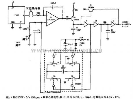
FM Broadcasting Circuit
Published:2011/5/17 3:27:00 Author:Michel | Keyword: FM, Broadcasting Circuit
View full Circuit Diagram | Comments | Reading(522)
light-operated series switches circuit
Published:2011/5/31 7:46:00 Author:chopper | Keyword: light-operated, series switches
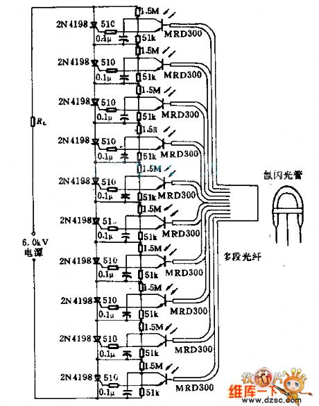
The light of xenon spark tube is transported to photistor MRD300 by optical fiber.The photosensitive electric current can trigger a series of thyristors after it is amplified,and offer load RL 6000V voltage.The manner of photoelectric trigger can eliminate the inductance delay generated by normal trigger's line.It requires that thyristors have the same risetime,so that can protect the circuit from triggering by those slowest inductive components.
(View)
View full Circuit Diagram | Comments | Reading(567)
Adjustable photoelectric isolation circuit
Published:2011/6/8 6:27:00 Author:chopper | Keyword: Adjustable, photoelectric isolation
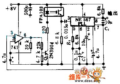
This circuit modulats(modulation frequency is about 1400HZ ) the optoelectronic isolator FPA103 produced by XianTong company and demodulates the singal from detector,in order to make optoelectronic not sensitive to fluorescent lamp light but not to decrease the performance.R1,C1 regulates the voltage controlled oscillator of PLL integrated circuit within 1400HZ around,741 operational amplifier converts the triangular wave of phase-locked loop into the square wave whose duty ratio is 50%,and drives the LED of optoelectronic isolator through Q1.
(View)
View full Circuit Diagram | Comments | Reading(613)
555 astable multivibrator circuit
Published:2011/5/25 1:01:00 Author:Christina | Keyword: astable multivibrator
As the figure shown, if you connect 555 (or 1/2 556) with three resistance, tolerance components, it is the astable multivibrator mode. The difference between the astable multivibrator mode and the monostabillity mode is: the astable multivibrator mode's trigger port (pin-2) connects to the C of the charging & discharging circuit, but not controlled by the output trigger. (View)
View full Circuit Diagram | Comments | Reading(895)
AD620 pre-amplifier circuit
Published:2011/5/25 1:01:00 Author:Christina | Keyword: pre-amplifier
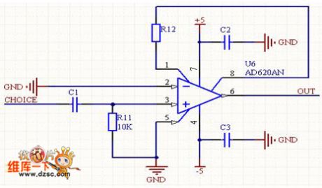
Because the string signal generator output signal's maximum value is about 1V, so the voltage drop of the sampling resistance which is connected with the network load needs to amplify the sampling signal. This circuit uses the two stages amplifier, and the preamplifier stage uses the AD620.
Figure: AD620 pre-amplifier circuit
The AD620 is designed as one kind of low power consumption amplifier, and it can be used as the small signal's pre-amplifier stage, the signal which is amplified by AD620 has small distortion. (View)
View full Circuit Diagram | Comments | Reading(4827)
Single variable dual-supply ciruit
Published:2011/6/1 21:11:00 Author:Christina | Keyword: Single variable, dual-supply
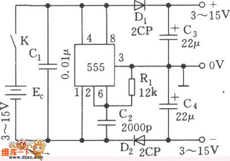
As the figure shows, the astable multivibrator is composed of the 555 and R1, C2, the oscillation frequency is about 20kHz, and the charging and discharging time constants are R1C2, so the duty ratio is 50%. The output 20kHz pulse wave is rectified and filtered by the D1, C3 and D2, C4, so the circuit outputs the ±EDD dual-power-supply. It uses the double time bases 555 to improve the load current to 50 mA. (View)
View full Circuit Diagram | Comments | Reading(1999)
Low Noise 20MHz Wideband Amplification Circuit
Published:2011/5/17 5:44:00 Author:Robert | Keyword: Low Noise, 20MHz, Wideband, Amplification
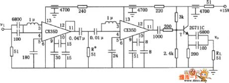
The Low Noise 20MHz Wideband Amplification Circuit is shown in the picture in the picture. This wideband amplification is made up by two CX35D, and its main technical specifications is: bandwidth 10~200MHz; when RL=500Ω the voltage gain is Av>=80; the undistorted output is Vo>=500mV, andthe short noise is less than 40uV for the equivalent toinput port.
(View)
View full Circuit Diagram | Comments | Reading(528)
light-emitting diode voltage measurement circuit
Published:2011/5/11 3:16:00 Author:Christina | Keyword: light-emitting diode, voltage measurement
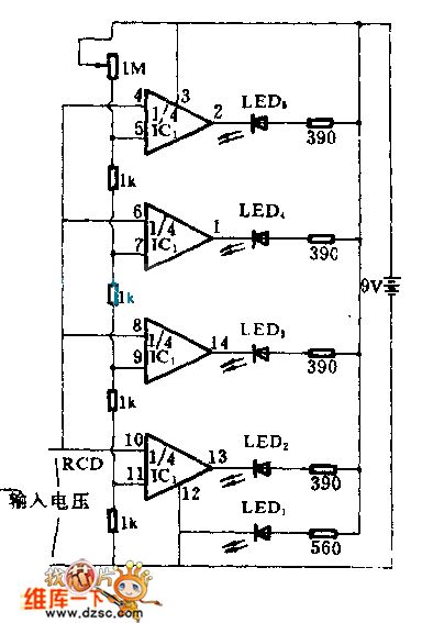
This circuit uses the LED to indicate (View)
View full Circuit Diagram | Comments | Reading(757)
Pressurization transform power supply circuit with the frequency automatic offset features composed of the MAX630
Published:2011/5/25 19:20:00 Author:Christina | Keyword: Pressurization, transform, power supply, frequency, automatic offset
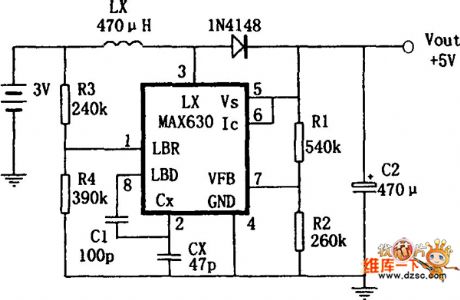
The low voltage frequency offset pressurization transform power supply which is composed of the MAX630's low battery voltage detection function is as shown. The feature of this circuit is: when the battery voltage is lower than nominal value (3V), about 2V, this circuit can highly efficiency (85%) supply the 40mA,5V DC voltage at the output port. The process is: the battery voltage drops, and causes the voltage of MAX630's pin1 (from the R3 and R4's separate pressure of the battery electric) todrop too, when the voltage is lower than the battery voltage detection comparator's threshold voltage (1.31V), the detection output port (pin-8) LBD becomes the low-level voltage, this connects the C1 together with the Cx and reduces MAX630 internal oscillator's frequency.
(View)
View full Circuit Diagram | Comments | Reading(596)
Logic level by NE555 and MOSFET interface circuit
Published:2011/6/9 21:20:00 Author:John | Keyword: Logic level, MOSFET interface
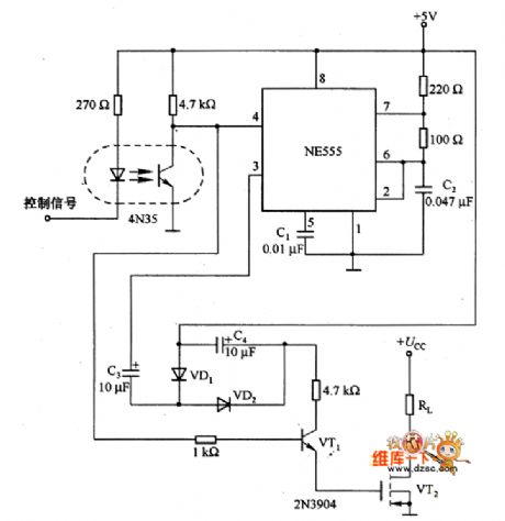
In the circuit, NE555 is the non-steady-state multivibrator with oscillation frequency of 70KHz. Control input signals by reset pin (pin 4) on / off controls its state of oscillation. When pin 4 inputs high electricity, the oscillator starts to work. When pin 4 inputs high electricity, the oscillation stops. Output of NE555’s pin 3 provides input voltage for dual-voltage rectifier circuit composed of VD1, VD2, C3 and C4. And the output of dual-voltage rectifier circuit is 8•5V. Digital logic control signal is added to NE555’s reset pin (pin 4) through the optical coupler 4N35. The optical coupler would do electrical isolation between the digital logic control signal and the high load.
(View)
View full Circuit Diagram | Comments | Reading(2286)
AC photoelectric switch circuit
Published:2011/5/27 7:09:00 Author:John | Keyword: photoelectric switch
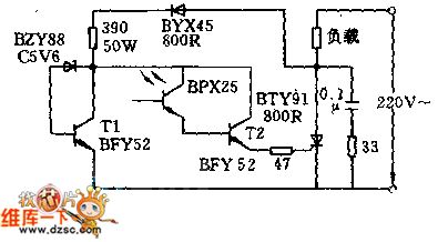
The circuit acts when the light intensity is over 700LX. . At this moment, the phototransistor BFY52 and transistor BPX25 trigger current to thyristor BTY91/800R. Where there is bright light on the phototransistor, the trigger pulse always occurs at each positive half cycle beginning of about 6 °. The maximum arithmetic average of load-through DC half-wave current is 16A.
Regulator BZY88/C5, transistor T1 and its connection resistor 390Ω form to limit the voltage in trigger circuit to not exceed 6V. Diode BYX45/800R is used to block the negative half-cycle grid voltage. The resistor 33Ω and capacitor 0.1μF are used to protect the thyristor against over-voltage.
(View)
View full Circuit Diagram | Comments | Reading(1014)
instrumentation amplifier with ±100 volt common mode range circuit
Published:2011/6/9 21:18:00 Author:John | Keyword: instrumentation amplifier
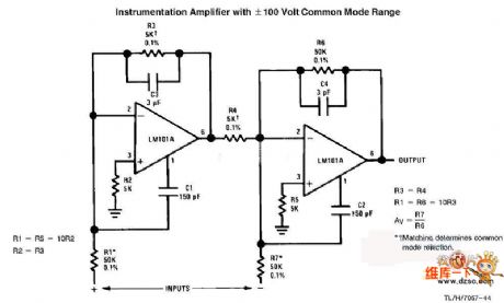
Instrumentation amplifier with ±100 volt common mode range circuit is shown below.
(View)
View full Circuit Diagram | Comments | Reading(897)
The OTL Earphone Amplifier composed of double triode ECC822 electronic value circuit diagram
Published:2011/6/2 21:11:00 Author:Sophia | Keyword: Double triode, ECC822electronic value, OTL Earphone Amplifier
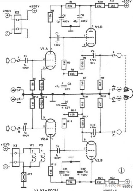
As shown, the curcuit is using the double triode equivalent of E802C、E82CC and North American12AU7 and domestic 6N10as amplifier, This kind of transistor is characterized by excellent indicator and long service life. HD head Amplifier will produce enough signal amplitude to drive earphone. Audions of base pin 1,2,3 amplify signal. Input signal arrives circuit board through 50kΩvolume control logarithmic potentiometer p1(p1 is not shown in the diagram), and pass C1、R1 to input to pre-amplification. meanwhile,R1、C1l must provide indispensible negative grid bias. Gain is decided by R8, and maximum input voltage is determined by R2. R9 is to determine that static anode current is in utmost linear part of characteristic curve. The input signal amplified by phase reversal in positive pole arrives the second stage grid through C2 coupling.The second stage cathode resistance is divided to R5 and R6. R5 and R6 connect in series to form load resistance.
(View)
View full Circuit Diagram | Comments | Reading(807)
The high voltage input FET power amplifier circuit diagram
Published:2011/6/10 22:01:00 Author:leo | Keyword: The high voltage input FET power amplifier circuit diagram, 2SA639, 2SC1279, 2SA818, 2SA633, 2SC1628
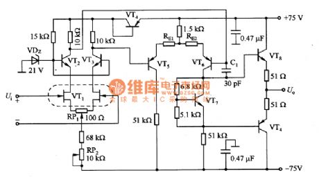
As the picture 1 shows, it is a high voltage input power amplifier circuit. The input VT1 of the circuit adopts FET tube. And its drain is connected to common base amplifier formed by VT2 and VT3, which is used to electric level move in order to prevent high voltage from being connecting to the drain of VT1. VT5 and VT6 are differential amplifying circuit.When the emitter is connect is added the current feedback, convert rate will be improved. Feedback resistance value of RE1 and RE2 need to be 0 to 5OOΩ. VT4 should be connected to be a diode which is used to make up the difference of UBE of VT5 and VT^ causing by temperature changes. VT8 and VT9 are push-pull output circuit. (View)
View full Circuit Diagram | Comments | Reading(4650)
| Pages:199/250 At 20181182183184185186187188189190191192193194195196197198199200Under 20 |
Circuit Categories
power supply circuit
Amplifier Circuit
Basic Circuit
LED and Light Circuit
Sensor Circuit
Signal Processing
Electrical Equipment Circuit
Control Circuit
Remote Control Circuit
A/D-D/A Converter Circuit
Audio Circuit
Measuring and Test Circuit
Communication Circuit
Computer-Related Circuit
555 Circuit
Automotive Circuit
Repairing Circuit