
Index 183
CXA8008P-Single chip player integrated circuit
Published:2011/7/10 5:53:00 Author:leo | Keyword: Single chip, dual channel
CXA8008P is a kind of single chip player integrated circuit produced by Sony Company. The hot product ANYTECH20 player in the market is made up of this component.
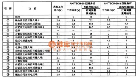
1.CXA8008P inner circuit diagram and pin functions:
CXA8008P is dual channel single chip player circuit. Every channle contains a fronted amplifier, DC volume control circuit and power amplifier. Its inner circuit diagram is shown in the picture 1. This IC uses 18 pin dual line package and its pin functions are shown in the picture 1.
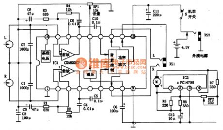
2. CXA8008P classic applying circuits.
Its classic applying circuits are shown in the picture. (View)
View full Circuit Diagram | Comments | Reading(2181)
USB switching to RS232 dual serial port circuit
Published:2011/7/7 7:21:00 Author:Fiona | Keyword: dual serial port
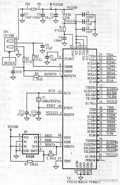
It needs to pay attention to the following points when designing:First of all:the resistance of the FT2232C's USBDP,USBDM two input terminals' resistors must be equal,the typical value is 27Ω, and the resistors must be 1% precision resistors,otherwise they easily lead to input impedance mismatch so that the circuit can not work normally.Secondly,at both ends of the 2 the capacitance of two capacitors which are at both ends of the circuit oscillator must be equal too, typical value is 27pF.Due to the design requirement is to get 2 serial port, thus extrapolated EEPROM can not answer, but directly connect the EEDATA terminal of FT2232C to VCC by 10kΩ resistor.
(View)
View full Circuit Diagram | Comments | Reading(901)
Controlled by single chip DC brushless motor driver and interface circuit
Published:2011/7/8 2:42:00 Author:Fiona | Keyword: Controlled by single chip, DC brushless motor, driver and interface
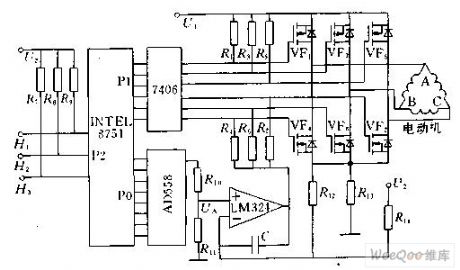
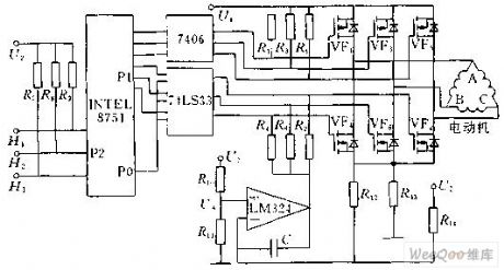
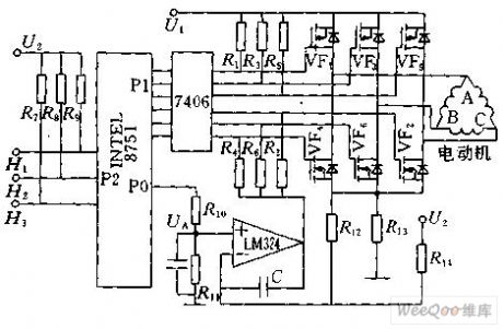
Figure 1 shows the functional block diagram of using 8751 single chip to control the brushless DC motor.8751's P1 is connected with the 7406 inverter control to control the brushless DC motor commutation,P2 is used for measuring the signal H1, H2, H3 from position sensor,P0 externally connects a digital to analog converter.According to the commutation of stator windings, first it needs to find the state of three rotor magnet position sensor signals H1,H2,H3 and the relationship between 6 power tubes,then it puts the information in tabular form to the single-chip's EEPROM.
(View)
View full Circuit Diagram | Comments | Reading(3046)
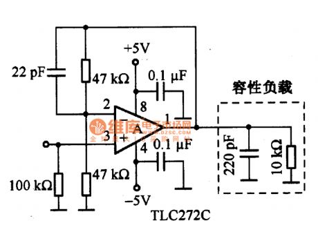
CMOS Operational amplifier inphase amplifier circuit diagram
Published:2011/6/14 7:58:00 Author:Sophia | Keyword: CMOS Operational amplifier, inphase amplifier
(View)
View full Circuit Diagram | Comments | Reading(679)
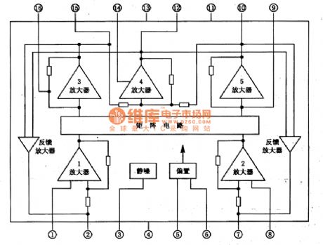
Internal Block Circuit Diagram of IC LA445
Published:2011/7/7 8:39:00 Author:Vicky | Keyword: Internal Block Circuit Diagram
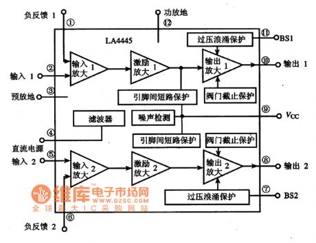
LA445 is a dual-channel audio power amplifier integrated circuit produced by Japanese SANYO Electric. It is widely used in home audio device, vehicle audio device, television audio system, and computer audio System.
Functions and Features
IC LA445 consists of dual-channel audio power amplifier circuit, short-circuit protection circuit, overvoltage protection circuit, surge suppressor circuit, and thermal cutoff circuit. It has various features, such as strong restraining capacity of ripple wave, high separating degree, good balance, and convenient assembling of radiator. It can constitute dual-channel or BTL power amplifier.
The limit working voltage of IC L445 is 25V, maximum quiescent current is 100mA, and typical value is 75mA. Its internal block circuit diagram is shown in the picture. (View)
View full Circuit Diagram | Comments | Reading(1442)
TA8256BH audio power amplifier integrated circuit
Published:2011/7/6 6:06:00 Author:chopper | Keyword: audio power amplifier, integrated circuit
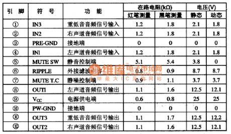
TA8356BH is a new audio power amplifier integrated circuitproduced by Company Toshiba,and it is applied to audio equipment, the multimedia sound,TV acoustics and so on.1.Function characteristics TA8256BH integrated circuits contains three-way audio power amplifier circuit, mute control circuit, and other auxiliary functions circuit. 2 function and data of pins TA8256BH IC adopts 12-pinned single in-line package,and it is used in large-screen TV of Haier Body Strong 34F9BT-TD series, its function and data of pins of the IC are listed in Chart 1.
(View)
View full Circuit Diagram | Comments | Reading(1048)
QS6M3 internal circuit
Published:2011/7/6 9:07:00 Author:John | Keyword: internal circuit
View full Circuit Diagram | Comments | Reading(587)
MAX809 reset circuit
Published:2011/7/4 0:35:00 Author:John | Keyword: reset
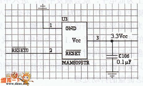
In the SCM system, MCU needs reset circuit, which can use R-C reset circuit or reset circuit achieved by reset chip. R-C reset circuit is economic. But it is not ratherreliable. The reset circuit achieved by reset chip is with high reliability. Therefore, in order to ensure the reliability of reset circuit, the system uses reset circuit achieved by reset chip. The system uses a MAX809 chip. And reset circuit is as shown below.
In order to reduce the interference of power supply, a 0.1μF capacitor is also needed to be placed on a reset chip's power input legs. Such can achieve the filtering and reduce disruption of the input end.
(View)
View full Circuit Diagram | Comments | Reading(837)
TA8106F double track headset drive integrated circuit
Published:2011/7/5 5:45:00 Author:chopper | Keyword: double track, headset drive, integrated circuit
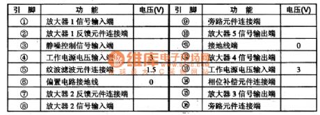
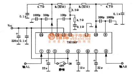
TA8106F is a dual track headset drive integrated circuit produced by Toshiba Company,and it is applied to mini,thin radio or cassette and recording radio as low-power drive circuit.1.The inner circuit and function of pins of TA8106FThe inner circuit of TA8106F integrated package includes two audio preamplifier premagnification circuits of same function,matrix power drive circuit,squelch circuit,biasing circuit,feedback amplifier circuit and so on.The inner circuit of the integrated package is shown as picture 1.This IC adopts dual inline 16 pinned flat package.
(View)
View full Circuit Diagram | Comments | Reading(1183)
TA75558P wide band with double operational amplifiers circuit
Published:2011/7/5 1:12:00 Author:chopper | Keyword: wide band, double operational amplifiers
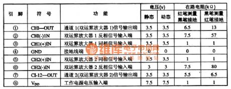
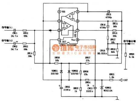
TA75558P is a wide band with double operational amplifiers circuit produced by company TOSHIBA.This IC is applied to the acoustic circuit as comparator or active low-pass filter.1.The inner circuit and function of pins of TA75558PThe inner circuit and typical application circuit of TA75558P integrated package are shown as picture 1.This IC adopts dual inline 8 pinned package.Its function and data of pins of the integrated circuit are shown as chart 1.
2.The typical application circuit of TA75558PTA75558P can be taken as active low-pass filter,The typical application circuit of its integrated package is shown as picture 1.
(View)
View full Circuit Diagram | Comments | Reading(2076)
QS5U21 and QS5U23 internal circuit
Published:2011/7/6 9:09:00 Author:John | Keyword: internal circuit
View full Circuit Diagram | Comments | Reading(560)
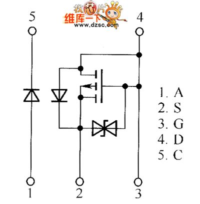
STV9379 field scanning output integrated circuit
Published:2011/6/28 3:13:00 Author:chopper | Keyword: field scanning, output, integrated circuit
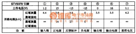
STV9379 is a special field scanning output integrated circuit and it is applied to Sony large-screen color TV widely as well as cassette mechanism large-screen color TV made in China of Sony cassette mechanism.1.function characteristicsSTV9306 integrated circuit includes field scanning output driving circuit,field scanning output circuit,voltage reference providing circuit,and other miscellaneous function circuit.2.function and data of pinsSTV9306 integrated circuit uses positive and negative power supply and adopts 7 pins single inline package and the function and data of pins of the integrated circuit are shown as chart 1.
(View)
View full Circuit Diagram | Comments | Reading(776)
MC1563 audio power amplifier circuit
Published:2011/7/5 1:14:00 Author:chopper | Keyword: audio, power amplifier
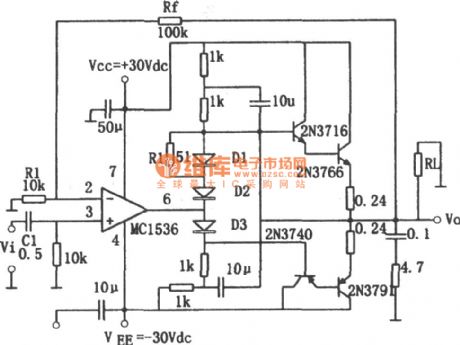
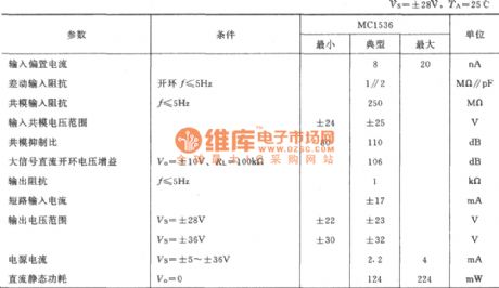
Figure shows the audio power amplifier. The circuit uses a high-voltage, internally-compensated integrated operational amplifier MC1536 .When the supply voltage Vs = ± 36V, the swing amplitude of output voltage is up to ± 30V, the maximum available supply voltage is up to ± 40V, input bias current is small (about 20nA below).The input offset current is less than 3nA, open-loop differential-mode gain is up to 5 × 10⁶ (typical value). The chip is suitable for low-frequency amplification.
(View)
View full Circuit Diagram | Comments | Reading(1001)
Calendar and clock display interface circuit
Published:2011/7/2 0:23:00 Author:Fiona | Keyword: Calendar and clock, display interface
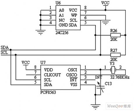
As shown in figure,this display interface is composed of EEPROM24C256 and calendar clock chip PCF8563.24C256 is a low voltage, serial interface and 256K capacity memorizer which is used for storing the measured blood pressure values.PCF8563 is a industrial multi-functional clock/calendar chip containing the I2C bus with very low power consumption which is introduced by PHILIPS company. It used for providing the time and date of blood pressure measurement so that it can be used and inquired afterwards.It is convenient for users to have a clear memory for their period blood pressure.It is practical and overcome the shortage of some electronic sphygmomanometer.
(View)
View full Circuit Diagram | Comments | Reading(1194)
The interface circuit of nRF2401 and CY7CS323
Published:2011/7/1 8:08:00 Author:Fiona | Keyword: interface circuit, mode
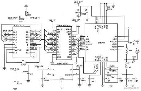
In the figure,CY7C63231 is 8-bit RISC microprocessor,it's especially suitable for the USB embedded side,the working voltage is 5V.nRF2401 is single-chip RF transceiver chip,it has four operating modes:send and receive mode,configuration mode,idle mode and off mode.All configuration,operating mode selection and sending and receiving are all completed through the control of CY7C63231's PO pin.It produces the working voltage (3.3 V) of nRF2401 by using voltage adjustment chip LP2980IM5-3.3,meanwhile,SN74LVC4245 produces 3.3 V control port and 5 V level translation, so that two kinds of chips can normally connect in different voltages.
(View)
View full Circuit Diagram | Comments | Reading(1844)
Interface circuit of LPC2200 and PDIUSBD12
Published:2011/7/1 7:19:00 Author:Fiona | Keyword: Interface circuit
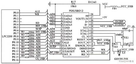
PDIUSBD12 uses the Bank2 part of LPC2200 external memory control,the data address is 0x82000000, the command address is Ox82000001. RST_USB, SUSP are the LPC2200's output pins, PDIUSBD) 12 interrupt signal is the interrupt input signal and an external interrupt O. C1, C2 and X1 offer PDIUSBD) 12 the clock input for the work.LED GoodLink flickers during normal communication.The AD0 of PDIUSBD12 is connected to the A0 of LPC2200,when the LPC2200 outputs 1 through the A0 pin, it shows that the data which outputs to the PDIUSBD12 data bus DO ~ D7 is command word; When the A0 pin outputs 0,it shows that the data which outputs to the PDIUSBD12 data bus DO ~ D7 is data word.
(View)
View full Circuit Diagram | Comments | Reading(1127)
The traditional RS485 interface circuit
Published:2011/7/1 22:57:00 Author:Fiona | Keyword: traditional RS485 interface
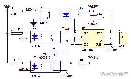
Used as a common communications interface devices, RS-485 / RS-422 chip can find corresponding models in many semiconductor companies, such as the ADI company ( device prefix is ADM).Most of the industrial RS-485 bus's customers should use the following circuit which connection is shown as the figure, this 485 circuit is mainly composed of 2 or 3 quick optocouplers,RS-485 transceiver device and isolating power supply module.Its advantages are simple connection and cheap price,its shortcomings are that using more device,big occupancy of the PCB area and thephotoelectric coupler is limited at the speed limit, power and LED aging.
(View)
View full Circuit Diagram | Comments | Reading(8758)
The instrument amplifier circuit with the transformer as the separator
Published:2011/7/1 21:18:00 Author:Borg | Keyword: instrument amplifier, transformer
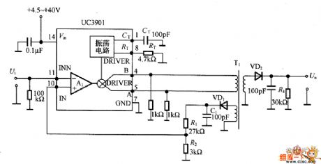
In the figure is the instrument amplifier circuit with the transformer as the separator, this is a circuit whose working voltage range is wide and the gains setting is easy. The input voltage is AM-modulated by UC3901 and added to the primary stage of the transformer T1, and then the input signal is recovered after it is detected by VD2 at the second stage. The modulating frequency of the circuit is decided by RT and CT, according to the parameter, which is 2MHz. The gain is AG=1+R2/1R=l+27kΩ/3kΩ=lO times. UC3901 is designed to be at the working state of the fault amplifier at the second stage of the switch stabilizer, whose working voltage range is +4.5~+40V.
(View)
View full Circuit Diagram | Comments | Reading(837)
The dual polarity input voltage/current separation amplifier circuit of transformer coupling type
Published:2011/7/4 4:01:00 Author:Borg | Keyword: dual polarity, voltage/current separation, transformer coupling
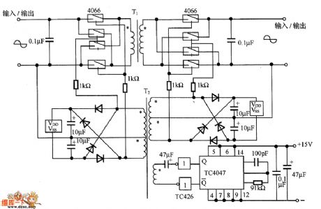
In the figure is the dual polarity input voltage/current separation amplifier circuit of transformer coupling type. In the circuit, DC/DC converter is in the same pattern with the FET chopper, the circuit adopts the analog switch 4066 to replace FET as the chopper, 4066 is connected as a bridge circuit which separates the signals by the transformer T1, as the circuits on the primary stage are the same, therefore, it has the function of dual-way input. Besides, with the positive/passive power supply driving the analog switch 4066, the forward/backward signals can be processed in the power supply voltage range.
(View)
View full Circuit Diagram | Comments | Reading(991)
The photoelectric coupling separation amplifier circuit of push-pull circuit improvement
Published:2011/7/4 20:04:00 Author:Borg | Keyword: photoelectric coupling, amplifier, push-pull circuit
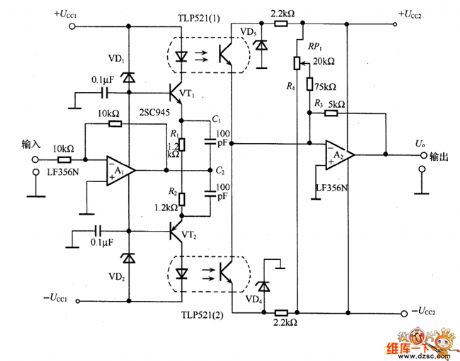
See as the figure, this is the photoelectric coupling separation amplifier circuit of push-pull circuit improvement: the forward current of the LED in the coupler is not in total proportion to the transistor electrode current, therefore, TLP521(1)and TLP521(2)are used to fulfill the push-full function in the circuit, the input and output feature of the 2 lines are integrated. A1 is the phase reverser, whose output voltage changes the emitting pole currents of VT1 and VT2, the LED is connected with its collecting electrode. The output voltage is converted into the forward bias current according to the input voltage, i.e constant current drive.
(View)
View full Circuit Diagram | Comments | Reading(931)
| Pages:183/250 At 20181182183184185186187188189190191192193194195196197198199200Under 20 |
Circuit Categories
power supply circuit
Amplifier Circuit
Basic Circuit
LED and Light Circuit
Sensor Circuit
Signal Processing
Electrical Equipment Circuit
Control Circuit
Remote Control Circuit
A/D-D/A Converter Circuit
Audio Circuit
Measuring and Test Circuit
Communication Circuit
Computer-Related Circuit
555 Circuit
Automotive Circuit
Repairing Circuit