
Index 191
The wireless reception headphone circuit
Published:2011/6/24 21:57:00 Author:qqtang | Keyword: wireless, reception, headphone
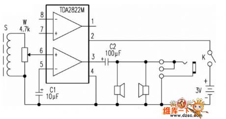
TDA2822-B-B wireless reception headphone is the tool that students receive the teaching audio. The writer has drawn a physical map, which is shown in the figure as reference.
See as the figure, TDA2822M is the dual-channel audio amplifier integrated circuit (in the figure there is one channel). The magnet coil S receives the audio signal from the audio classroom, the signal is sent to the 6-pin of the chip by the central head of potentiometer W, and then it is amplified and output by 3-pin, finally, it passes the coupling capacitor C2 and is added on the headphones in parallel connection, so the headphone is making sounds. (View)
View full Circuit Diagram | Comments | Reading(1206)
The timing circuit composed of the 555(ICM7555)of CMOS
Published:2011/6/25 21:32:00 Author:qqtang | Keyword: timing circuit, 555
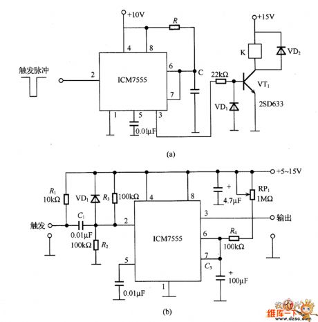
In the figure is the timing circuit composed of the 555(ICM7555)of CMOS, as CMOS is used, the impedance is very high, therefore, the amplitude of the time can be expanded largely, for example, it can compose a timer of several minutes. Here, figure (a) is the simple timing circuit.
In Figure (b) is a timing circuit which can set the time of 10~100s, in the circuit, to use to differential pulse trigger, the capacitor C1 is used for coupling, only when the voltage of 2-pin is lower than 1/3 of the power supply is the trigger motivated. The time is decided by C3 and R4+RP1. (View)
View full Circuit Diagram | Comments | Reading(1578)
20W OCL power amplifier circuit
Published:2011/6/13 8:31:00 Author:Christina | Keyword: 20W, OCL, power amplifier
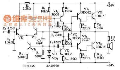
The circuit is as shown in the figure. The feature of the OCL power amplifier: the speaker is directly coupled with the output port of the amplifier. The circuit uses the positive and negative symmetrical power supply and the differential amplifier as the input port that can guarantee the zero DC potential, so it has good fidelity. The VT1 and VT2 can use the S3DG6 differential geminating tube.
Figure The 20W OCL power amplifier circuit
(View)
View full Circuit Diagram | Comments | Reading(4103)
Radio intermediate frequency amplifier circuit
Published:2011/6/13 8:20:00 Author:Christina | Keyword: Radio, intermediate frequency, amplifier
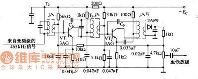
The intermediate frequency amplifier circuit of the general semiconductor radio is as shown. The 465kHz intermediate frequency signal which is produced by the frequency changing circuit is sent to the VT2 by the secondary stage of the intermediate frequency transformer T2 to be amplified, the amplification signal is sent to VT3 by the T3 intermediate frequency transformer to be amplified again, then it is sent to the wave detector by the T4 intermediate frequency transformer to be detected, the detected signal is sent to the low frequency amplification stage to be amplified.
The CN is the neutralizing capacitance of the circuit that can be used to inhibit the intermediate frequency parasitic oscillation.
Figure The radio intermediate frequency amplifier circuit
(View)
View full Circuit Diagram | Comments | Reading(1942)
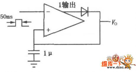
The 555 basic timing circuit
Published:2011/6/24 23:14:00 Author:qqtang | Keyword: basic timing
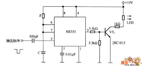
In the figure is the 555 basic timing circuit. In the circuit, if we add a figured trigger pulse on the 2-pin of 555, the 3-pin will output a intermittent pulse, the interval time is T≈RC. After being amplified by VT1, the signal drives the relevant circuit, such as the LED in the figure.
(View)
View full Circuit Diagram | Comments | Reading(651)
TV antenna amplifier circuit
Published:2011/6/13 8:05:00 Author:Christina | Keyword: TV, antenna, amplifier
The TV antenna amplifier circuit is as shown, the input loop is composed of the L1 and C1, and it plays the frequency selection and the impedance matching function. The first level of the amplifier uses the common emitter - common base amplifier circuit, this kind of circuit has the advantages of high stability and small noise coefficient. The second and third stages of the amplifier are the common emitter circuit, each stage has the tuning circuit. In order to make the amplifier to have the wide pass band, the tuning circuit uses the staggered tuning and adds the resistances R14, R6 and R10 in the oscillation loop. The potentiometer RP1 can be used to adjust the gain of the amplifier.
Figure 15-41 The circuit of the TV antenna amplifier
(View)
View full Circuit Diagram | Comments | Reading(3733)
The amplifier circuit with wide input voltage range
Published:2011/6/20 9:21:00 Author:Nancy | Keyword: wide input voltage range , amplifier circuit
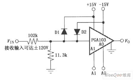
The circuit shown is a wide input range amplifier composed by PGA103. The 11.3kΩ and 102kΩ resistors form the voltage division circuit, the divider ratio is about 1/10, when the input voltage is 120V, the voltage added to PGA103 input after division is only 12V, therefore wide voltage input is available. Meanwhile, didoe D1, D2(1N4148) use as two-way clamp, making the input voltage of PGA103 ±15 to 士0.7V. (View)
View full Circuit Diagram | Comments | Reading(780)
Differential amplification basic circuit
Published:2011/6/14 1:19:00 Author:Christina | Keyword: Differential amplification, basic circuit
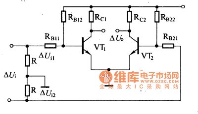
The differential amplification basic circuit is as shown in the figure. It is composed of two single tube amplifier circuit with the same parameters. The resistances of RB11 and RB22 are the same, they are the current-limiting resistance of the input circuit; the resistances of RB21 and RB22 are the same, they are the biasing resistor; the resistances of Rc1 and RC2 are the same, they are the collector load resistor; R is the pressure equalizing resistance of the input port, it is also the under bias resistor. The signal is input from the base electrodes of VT1 and VT2, and the signal is output from the collectors of VT1 and VT2, so this circuit has two input ports and two input ports.
The differential amplifier circuit has the high magnification to the differential mode signal, and it also has the strong inhibiting effect to the mode signal, so it solves the contradiction between the amplification and zero drift perfectly.
Figure The differential amplification basic circuit
(View)
View full Circuit Diagram | Comments | Reading(729)
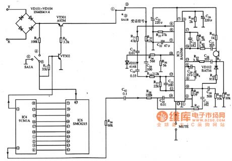
BA6566 call integrated circuit
Published:2011/6/14 1:31:00 Author:Christina | Keyword: call, integrated circuit
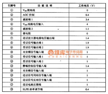
The BA6566 is designed as one kind of call integrated circuit that can be used in the Panasonic series telephone.
1.Pin functions and data
The BA6566 integrated circuit is in the 18-pin dual-row DIP package, the pin functions and data is as shown in table 1.
Table The pin functions and data of the BA6566
2.Typical application circuit
The call system typical application circuit which is composed of the BA6566 is as shown in figure 1.
Figure 1 The call system typical application circuit which is composed of the BA6566
(View)
View full Circuit Diagram | Comments | Reading(1909)
wideband amplifier circuit with 600v/us conversion speed
Published:2011/6/18 10:46:00 Author:Nancy | Keyword: wideband amplifier, 600v/us conversion speed
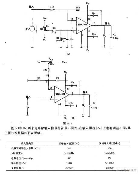
Circuit (a) and (b) has various difference at input impedance |Ze| except that the symbol of the input signal is not the same. (View)
View full Circuit Diagram | Comments | Reading(616)
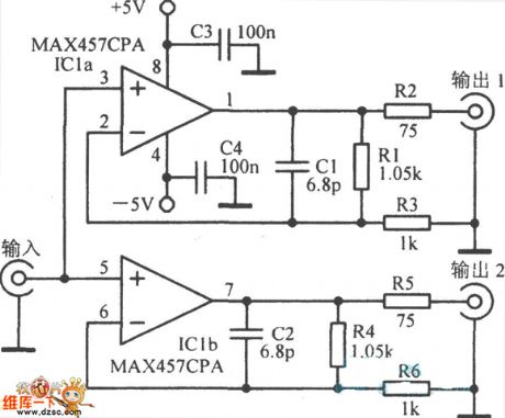
The high speed gain auto-converting amplifier circuit
Published:2011/6/25 4:31:00 Author:qqtang | Keyword: high speed, auto-converting amplifier
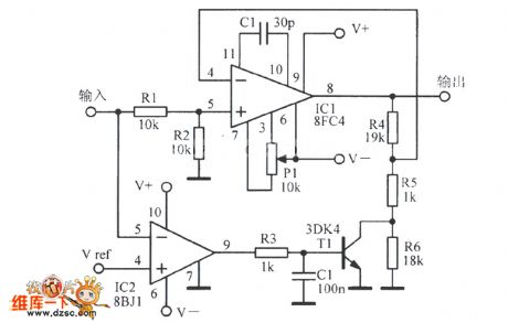
The high speed gain auto-converting amplifier circuit is shown in the figure.
(View)
View full Circuit Diagram | Comments | Reading(638)
LM161, LM1261 and LM1361--the high speed compensation voltage comparator circuit
Published:2011/6/25 4:45:00 Author:qqtang | Keyword: high speed, compensation, voltage comparator
LM161/261/361 have a high transmitting speed, a general power supply voltage, separated strobe terminals and two compensatory output TTL signals of little time delay. Its input distortion voltage is low. When it is driven, its rotating speed is low. It is in dual in-line package. In the figure is the high speed value wave detector.
(View)
View full Circuit Diagram | Comments | Reading(737)
SN55451B and SN75451B--the dual perpheral forward AND driver circuit
Published:2011/6/25 5:03:00 Author:qqtang | Keyword: dual, perpheral, forward driver
SN55451B/75451B is theAND logic periphery driver whose input terminal is compatible with TTL or DTL, its input current is 300mA, its input voltage is high, and its rotating speed is high. Its typical application circuit is shown in the figure.
(View)
View full Circuit Diagram | Comments | Reading(700)
The dual periphery forward OR driver circuit
Published:2011/6/25 5:02:00 Author:qqtang | Keyword: dual periphery, forward, OR driver
SN55453B/75453B is the OR logic periphery driver whose input terminal is compatible with TTL or DTL, its input current is 300mA, its input voltage is high, and its rotating speed is high. Its typical application circuit is shown in the figure.
(View)
View full Circuit Diagram | Comments | Reading(694)
SN55452B and SN75452B--The dual periphery forward NOR driver circuit
Published:2011/6/25 5:06:00 Author:qqtang | Keyword: dual periphery, forward, NOR driver
75452B/SN55452Bis the NOR logic periphery driver whose input terminal is compatible with TTL or DTL, its input current is 300mA, its input voltage is high, and its rotating speed is high. Its typical application circuit is shown in the figure.
(View)
View full Circuit Diagram | Comments | Reading(645)
The dual-channel video amplifier circuit
Published:2011/6/25 5:08:00 Author:qqtang | Keyword: dual-channel, video amplifier
The dual-channel video amplifier circuit is shown as above.
(View)
View full Circuit Diagram | Comments | Reading(921)
TDA6120Q--the video output amplifier circuit
Published:2011/6/25 5:18:00 Author:qqtang | Keyword: video, output amplifier

TDA6120Q is a single video output amplifier of 32MHz and 125VP-P, which is in plastic DIL and curve SIL power package, its high voltage DMOS technology can drive the passive pole of the color CRT, it can be used in high definition TVs or monitors. TDA6120Q has the fast passive pole test output of the dark current circuit, when output signal is 60v (peak value), the small signal wide band is 47MHz(typical value). TDA6120Q has a high power PSRR, whose maximum gain is over 46dB. The pin arrangement and functions of TDA6120Q are shown in the figure.
(View)
View full Circuit Diagram | Comments | Reading(743)
Automatic transceiver & conversion RS-485 interface circuit and testing circuit
Published:2011/6/19 8:37:00 Author:TaoXi | Keyword: Automatic transceiver, conversion, interface circuit , testing circuit
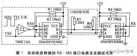
The interface circuit is as shown in the dotted line box of the figure 1, by analysising the true value table, the sending and receiving process are: when the sending port DI=O, the DE/RE=1 sends the 0 electrical level, the receiving port RO=O; when the sending port DI=1, DE/RE=0, VA=VB=2.5V, the receiving port RO=1 with the function of the pull-up resistor.
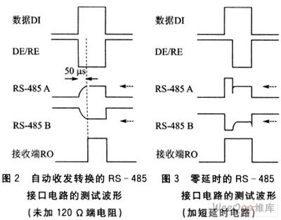
If you add the 1kHz TTL square wave at the TXo port of the interface circuit to test the circuit. The interface chip pin 485-A and pin 485-B all have the 50μs voltage changing process when you have not add the 120Ω port resistance, as the figure 2 shows. The receiving port Ro waveform's rising edge has the 30~40μs obvious delay to cause the large transmission error; when you add the 120Ω port resistance, the delay decreases, it is about 3μs.
(View)
View full Circuit Diagram | Comments | Reading(1110)
Single-chip microcomputer and LCD monitor button interface circuit
Published:2011/6/19 8:13:00 Author:TaoXi | Keyword: Single-chip microcomputer, LCD monitor, button interface
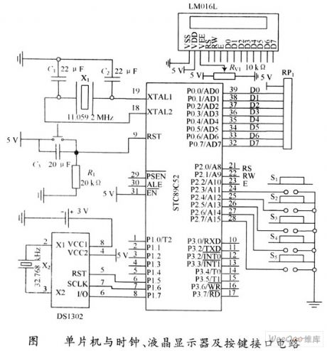
The interface circuit part of the single-chip microcomputer and the clock chip DS1302: the DS1302 is designed as one kind of high performance, low power consumption clock chip which is produced by the DALLAS company, this device uses the SPI three line interface to synchronously communicate with the CPU, and it supplies the second, the minute, the hour, the day, the week, the month and the year, when the month is less than 31 days, it can automaticly adjust, also it has the function of leap year compensation. The operating voltage is 2.5 to 5.5V, the application circuit is as shown in the figure.
The interface circuit part of the single-chip microcomputer and the LCD monitor: the data interface line of the LCD monitor is connected with the P0 port of the single-chip microcomputer. The P2.0, P2.1, P2.2 can be used in the operation of the LCD screen's reading and writing. The specific circuit is as shown in the figure.
(View)
View full Circuit Diagram | Comments | Reading(1917)
KRIDENT car subwoofer circuit
Published:2011/6/19 8:02:00 Author:TaoXi | Keyword: KRIDENT, car subwoofer
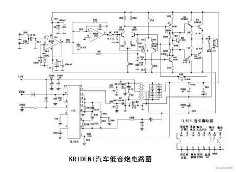
KRIDENT car subwoofer circuit (View)
View full Circuit Diagram | Comments | Reading(4462)
| Pages:191/250 At 20181182183184185186187188189190191192193194195196197198199200Under 20 |
Circuit Categories
power supply circuit
Amplifier Circuit
Basic Circuit
LED and Light Circuit
Sensor Circuit
Signal Processing
Electrical Equipment Circuit
Control Circuit
Remote Control Circuit
A/D-D/A Converter Circuit
Audio Circuit
Measuring and Test Circuit
Communication Circuit
Computer-Related Circuit
555 Circuit
Automotive Circuit
Repairing Circuit