
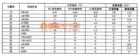
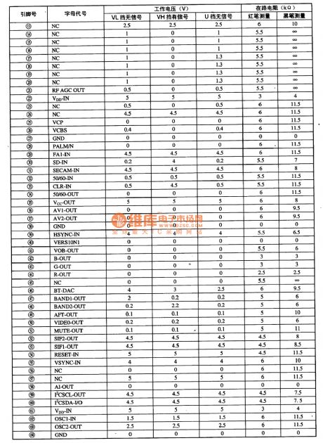
Index 190
IF amplifier IC circuit
Published:2011/6/19 4:47:00 Author:John | Keyword: IF amplifier
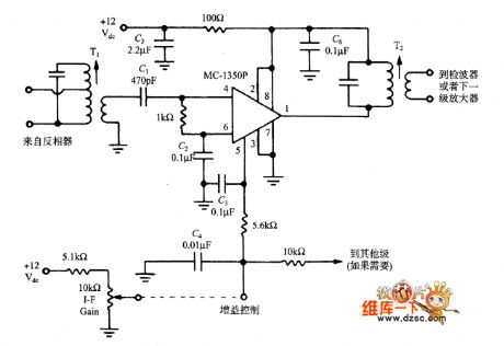
The picture shows a basic circuit composed of IF amplifier module. If a local reception of AM receiver is needed, the first-level circuit is only needed. For receivers with short-wave or other needed high-sensitivity, two or three circuits are needed to increase the gain. Each level of the gain requires 50dB and some projects may require 80 ~ 110dB.
IF amplifier module is constructed based MC-1350P gain module chip (the chip can also replace NTE-746 in the NTE). (View)
View full Circuit Diagram | Comments | Reading(2037)
The receiving party modem and single-chip microcomputer interface circuit
Published:2011/6/23 21:14:00 Author:TaoXi
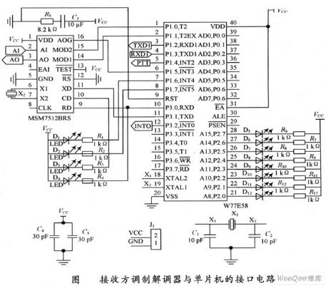
The receiving party modem circuit and the battlefield sensor modem circuit have the same using and control methods in the single-chip microcomputer and the demodulation chip. The different is the second serial port of the single-chip microcomputer is connected with the RS 232C port of the computer through the level conversion circuit, it sends the received digital signal to the PC. The receiving party modem and single-chip microcomputer interface circuit is as shown in the figure. The D1~D8 are the receive data display, the D9 is the system power indicator, the D10 is the correct sending indicator, the D11 is the carrier wave detection indicator, the D12 is the data transmission indicator.
(View)
View full Circuit Diagram | Comments | Reading(618)
The phase-lock loop frequency doubler (9316)
Published:2011/6/17 7:46:00 Author:Borg | Keyword: phase-lock loop, frequency doubler
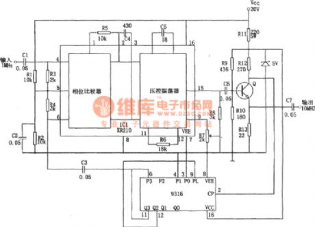
In the circuit is the phase-lock loop frequency doubler. This circuit can switch the 1MHz standard frequency into the 10MHz reference frequency, and the stability and precision of the output frequency are the same with the 1MHz standard frequency. The PLL integrated circuit in the circuit is XR210. The 1MHz reference signal is coupled on the 4-pin of IC1 by capacitor C1, and the output signal of the counter 9316 is added on the 6-pin, they are compared by the phase comparator inside IC1. The output of the phase comparator is filtered by capacitor C4. (View)
View full Circuit Diagram | Comments | Reading(750)
The headphone amplifier circuit (triode + op-amp opa2134)
Published:2011/6/26 20:59:00 Author:Borg | Keyword: headphone amplifier, op-amp
View full Circuit Diagram | Comments | Reading(3368)
The instrument amplifier circuit of the ordinary op-amp
Published:2011/6/27 19:46:00 Author:Borg | Keyword: instrument amplifier, op-amp
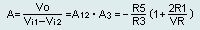
The circuit is in figure 1. The principle of the circuit is not complex. To make the circuit balanced, then R1=R2, R3=R4 and R5=R6, as the feature of each capacitor can't be the same, so on Pin1 and Pin of A1 and A2, we add the reset potentiometer of VR1 and VT2, which is practical in real application. We assume that all the mismatch, dissonance and current of A1 and A2 are 0, the DMV gain will be:
The whole circuit is powered by two teams of positive and passive power supplies, which can amplify the forward or backward voltage.
(View)
View full Circuit Diagram | Comments | Reading(784)
The low-noise ecc83 headphone amplifier circuit
Published:2011/6/26 8:27:00 Author:Borg | Keyword: headphone amplifier, low-noise
The low-noise ecc83 headphone amplifier circuit is shown as above.
(View)
View full Circuit Diagram | Comments | Reading(918)
The transistor bile taste sound adjusting circuit
Published:2011/6/27 10:27:00 Author:Borg | Keyword: transistor, bile taste
The transistor bile taste sound adjusting circuit is shown as above.
(View)
View full Circuit Diagram | Comments | Reading(694)
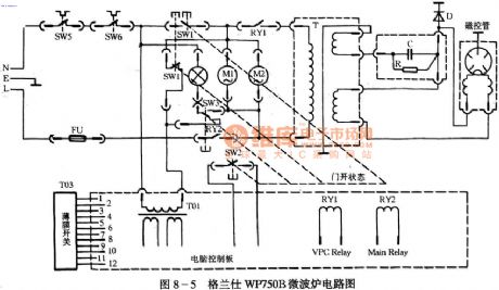
principle of Glanz microwave oven circuit
Published:2011/6/22 19:55:00 Author:chopper | Keyword: principle, Glanz, microwave oven
View full Circuit Diagram | Comments | Reading(2206)
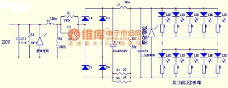
capacitive step-down driving LED circuit
Published:2011/6/22 19:59:00 Author:chopper | Keyword: capacitive, step-down, LED, driving
View full Circuit Diagram | Comments | Reading(699)
The FET pipe drive timing flash circuit
Published:2011/6/25 20:25:00 Author:qqtang | Keyword: FET pipe, timing flash circuit
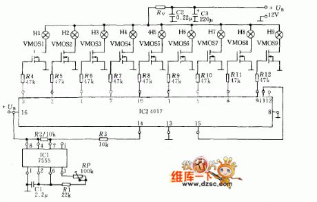
With the figured circuit, we can compose a circle light timing control circuit with a few elements. The circuit consists of the MOS time-base circuit 7555, CMOS decimal counter(pulse distributor) 4017 and end stage VMOS power transistor. The power transistor controls the bulb whose maximum current is 2A. The resistor RV between the bulb and the power supply +UH is used to limit the connected current.
The time-base frequency is adjusted by the potentiometer (about 0.5~10HZ). The 9 stage circling storage is controlled by the square wave output signal with the help of the clock. (View)
View full Circuit Diagram | Comments | Reading(684)
BH501 piano envelope door integrated circuit
Published:2011/6/13 20:22:00 Author:Christina | Keyword: piano, envelope door, integrated circuit
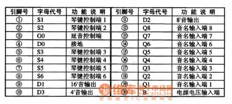
The BH5O1 is designed as one kind of piano envelope door integrated circuit that can be used with the BH2O0 series audio source integrated circuit, and it can be used to build up the high-grade keyboard such as the electronic piano, the electronic organ and other kinds of keyboards.
1.Pin functions
The BH501 is in the 20-pin dual-row DIP package, the pin functions is as shown in table 1.
Table 1 The pin functions of the BH501
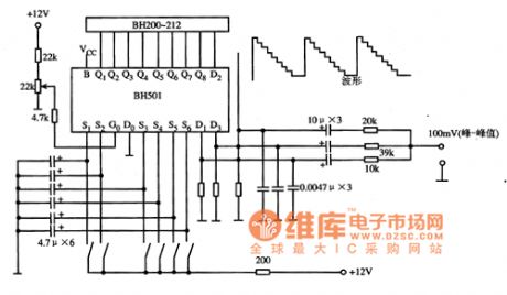
2.Typical application circuit
The typical application circuit of the piano envelope door which is composed of the BH501 is as shown in figure 1.
Figure 1 The BH501 typical application circuit
(View)
View full Circuit Diagram | Comments | Reading(1676)
MNI871675T6S--the single chip microcomputer integrated circuit
Published:2011/6/11 21:00:00 Author:qqtang | Keyword: single chip microcomputer, integrated circuit
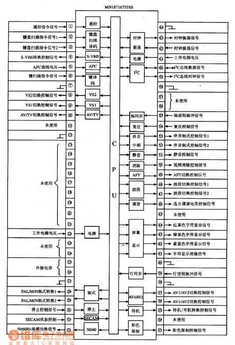
1.pin functions MNI871675T6S consists of the clock oscillating circuit, reset circuit,CPU, I2C general circuit, key scanning order decoder, system converting circuit, screen display, AV/TV shifting control circuit, and the other control and affiliated function circuit, etc.2.MNI871675T6S is in 64-pin dual in-line package, whose pin letter codes and data are listed in the table, and its internal circuit, pin functions and signal flow are shown in the figure.The pin letter codes and data of MNI871675T6S
(View)
View full Circuit Diagram | Comments | Reading(646)
Type B push-pull power amplifier typical circuit
Published:2011/6/13 9:40:00 Author:Christina | Keyword: Type B, push-pull, power amplifier, typical circuit
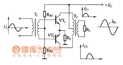
In order to improve the efficiency of the power amplifier and reduce the distortion, we usually use the type B push-pull power amplifier typical circuit. Features of the type B push-pull power amplifier typical circuit is: the static working point is in the starting part of the characteristic curve.
The typical circuit of the type B push-pull power amplifier typical circuit is as shown in the figure. From the circuit structure we know it is the symmetrical circuit which is composed of two unilateral power amplifier circuits. T1 is the input transformer which has the center tap in the secondary winding; T2 is the output transformer which has the center tap in the primary winding; VT1 and VT2 are the transistors which have the same parameters, and they can use the power amplifier geminating tube.
Figure The type B push-pull power amplifier typical circuit
(View)
View full Circuit Diagram | Comments | Reading(745)
The output angle test circuit composed of the regulator UZZ9000 and the reluctance sensor KMZ41
Published:2011/6/24 20:59:00 Author:qqtang | Keyword: output angle, regulator, reluctance sensor

The output angle test circuit composed of the regulator UZZ9000 and the reluctance sensor KMZ41 is shown in the figure, which is powered by the +5V power supply, and RP1~RP2 are the disorder voltage regulating potentiometer, RP3~RP4 are the gain adjusting potentiometer. R is the down resistor of the output terminal. The output voltage can be delivered to the digit voltmeter, indicating the value of the angle under test.
(View)
View full Circuit Diagram | Comments | Reading(937)
The precise pressure detection system circuit composed of the dual-channel intelligent sensor signal processor MAX1463
Published:2011/6/24 21:20:00 Author:qqtang | Keyword: pressure detection, dual-channel, signal processor
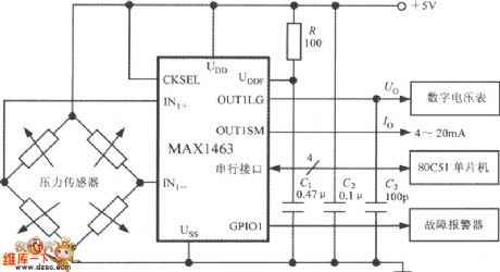
The output voltage of bridge pressure sensor is linked with the IN1+ and IN1- terminal of MAX1463. Under the control of CPU, the pressure signal is linearly adjusted, temperature-compensated and D/A converted, then it is delivered to the 80C51 single chip machine; it is also converted into the analog output voltage Uo by DAC and sent to the digital voltmeter, then the pressure value is indicated. The GPI01 pin of general D/A connector is connected with the fault alarm, when the wire of the sensor is broken or the CPU is overflowing while it is executing the programs, the buzzer is driven and rings.
(View)
View full Circuit Diagram | Comments | Reading(614)
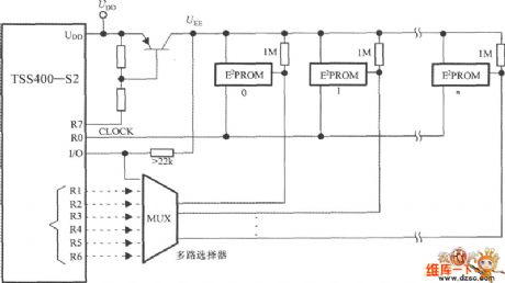
The connection circuit of the low-power programmable sensor signal processors of TSS400-S2 and E2PROM
Published:2011/6/25 20:59:00 Author:qqtang | Keyword: connection circuit, low-power, signal processors
View full Circuit Diagram | Comments | Reading(598)
Single tube RC coupling common emitter electrode amplifier circuit
Published:2011/6/13 9:22:00 Author:Christina | Keyword: Single tube, RC, coupling, common emitter electrode, amplifier
The circuit is as shown in the figure. This circuit can be used in the pre-amplifier stage of the low frequency small signal amplifier. The collector current Ic is 0.5~2mA, you can make the IC in the right position by adjusting R1.
Figure The single tube RC coupling common emitter electrode amplifier circuit
(View)
View full Circuit Diagram | Comments | Reading(1666)
The time delay pulse generating circuit based on the 220V and 50Hz AC
Published:2011/6/25 21:09:00 Author:qqtang | Keyword: time delay, pulse generating
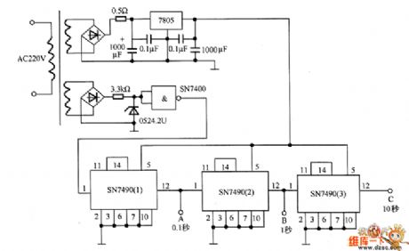
In the figure is the time delay pulse generating circuit based on the 220V and 50Hz AC. In the circuit, A pole can output the delayed pulse of 0.1s, B outputs 1s and C outputs 10s, all of which are the reference pulse circuit and also the basic circuit of the digital counter.
(View)
View full Circuit Diagram | Comments | Reading(1263)
Simple sound listening circuit
Published:2011/6/13 9:08:00 Author:Christina | Keyword: Simple, sound listening
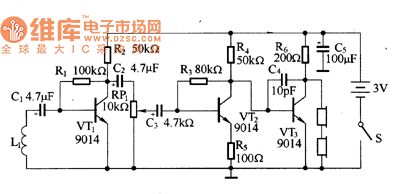
The simple sound listening circuit that can be used in teaching is as shown in the figure. The audio pre-amplifier circuit is composed of VT1, the two stages DC low low frequency amplifier circuit is composed of the VT2 and VT3. The L1 is the audio receiving coil, the low frequency signal which is inducted by the L1 adds to the amplifier circuit through C1 to be amplified, and the amplified signal is output by the headset. The RP1 can be used to adjust the volume.
Figure The simple sound listening circuit
(View)
View full Circuit Diagram | Comments | Reading(881)
The high stability pulse period gradual spread circuit
Published:2011/6/25 21:19:00 Author:qqtang | Keyword: high stability, pulse period
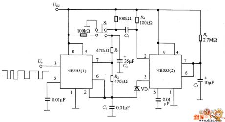
In the figure is the high stability pulse period gradual spread circuit. In the circuit, NE555(1) compose the pulse gradual spread timing circuit, NE555(2) compose the single steady trigger circuit, the NE555(1) and NE555(2) are connected by VD1. Before the key is pressed, the transistor inside NE555(2) is conducting, its 3-pin is outputting a low LEV, the diode VD1 is conducting and the voltage on capacitor C1 is 0, so the NE555(1) timer can't work.
When S1 is pressed, it will shake for some time. (View)
View full Circuit Diagram | Comments | Reading(1263)
| Pages:190/250 At 20181182183184185186187188189190191192193194195196197198199200Under 20 |
Circuit Categories
power supply circuit
Amplifier Circuit
Basic Circuit
LED and Light Circuit
Sensor Circuit
Signal Processing
Electrical Equipment Circuit
Control Circuit
Remote Control Circuit
A/D-D/A Converter Circuit
Audio Circuit
Measuring and Test Circuit
Communication Circuit
Computer-Related Circuit
555 Circuit
Automotive Circuit
Repairing Circuit