
Index 193
Product detector circuit
Published:2011/6/19 9:17:00 Author:John | Keyword: detector
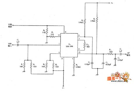
For SSB, it must be demodulated to recover the audio modulation. The circuit shown in the figure can get the job done well. It uses an LM-1496 double-balanced mixer as a product detector. This detector operates in CW, SSB and DSB signal (all of which need a local oscillator to inject signals). And audio signal can be generated by combining the local oscillator signal and the receiver’s SSB IF signal superheterodyne All of the SSB receivers use certain product detector in the end IF chain, many of which use some similar LM-1496 circuits just shown in the figure.
(View)
View full Circuit Diagram | Comments | Reading(2932)
6C16A headphone amplifier circuit diagarm
Published:2011/6/21 5:38:00 Author:Lucas | Keyword: headphone, amplifier
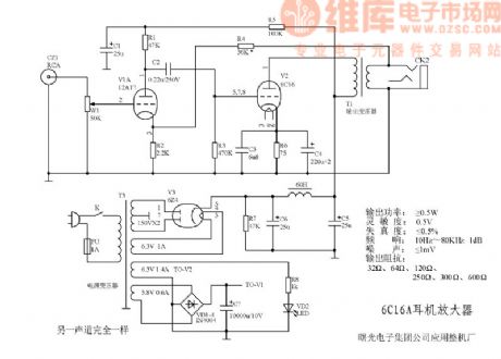
Output power: ≥ 0.5w; sensitivity: 0.5V; Distortion: ≤%; Frequency: 15Hz ~ 80KHz 1dB; noise: ≤ 1mV; output impedance: 32,64,120,250,300,600 Ω. (View)
View full Circuit Diagram | Comments | Reading(672)
Simple transistor IF amplifier circuit
Published:2011/6/17 9:49:00 Author:John | Keyword: transistor, IF amplifier
A simple IF amplifier is just as shown in the figure. AM band radio may have such a circuit, but FM receiver, shortwave receivers and other types of communications receivers may have two to four such circuits.
figure: Simple transistor IF amplifier circuit (View)
View full Circuit Diagram | Comments | Reading(3560)
SL56OC IF amplifier circuit
Published:2011/6/17 10:51:00 Author:John | Keyword: IF amplifier
A tuning circuit is as shown in the following. Tuned circuit T1 is used to replace the original input circuit. Output circuit is replaced with the transformer T2. Besides, V + terminal circuit here uses a Zener diode to rectifier the DC voltage.
figure: SL56OC IF amplifier circuit (View)
View full Circuit Diagram | Comments | Reading(800)
SL-560C IF amplifier circuit
Published:2011/6/17 10:46:00 Author:John | Keyword: IF amplifier
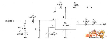
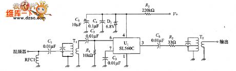
SL560C is basically a gain block that can be used in RF and IF frequency area. Figure shows a circuit based on SL560C. SL560C is the single-ended output circuit transferred by differential input. And the used input end needs to be set by the bypass of capacitor C3. Since this is a broadband circuit, the input or output circuit has no tuning function. The input circuit includes a 0.02μF input coupling capacitor and an RF choke (RFC1).
figure: SL-560C IF amplifier circuit (View)
View full Circuit Diagram | Comments | Reading(1495)
MC-1590 IF amplifier circuit
Published:2011/6/17 10:40:00 Author:John | Keyword: IF amplifier
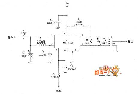
The picture shows the amplifier based on chips 1490 and 1590. The circuit can work well in the VHF region (30 ~ 80MHz). Input signal can be coupled to the IC through the capacitor C1. Tuning performance can be achieved by the parallel resonant circuit formed by C2 and L1. Capacitor C3 can apply the not used differential input end of chip 1590 to be AC grounded.
The output tuning reflects the differential output characteristics of chip 1590. As for LC tuned circuit, a parallel resonant circuit formed by the T1’s primary coil and capacitor C6 is connected between pin 5 and pin 6.
(View)
View full Circuit Diagram | Comments | Reading(2484)
Digital acquisition circuit
Published:2011/6/19 2:19:00 Author:John | Keyword: Digital acquisition
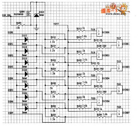
This system provides digital acquisition. Digital acquisition circuit is relatively simple and the concrete digital acquisition circuit is shown in the figure.
It can be seen from the figure, Q200 FET is used as a switch to start or stop collecting digital data acquisition. Circuit uses diodes for ESD protection. Digital's I or 0 is equivalent to the on –and-off of the circuit. Therefore, high and low electricuty on the digital capture input end can be generated, aiming to achieve digital collection tasks.
figure: Digital acquisition circuit (View)
View full Circuit Diagram | Comments | Reading(631)
Analog acquisition circuit
Published:2011/6/19 2:11:00 Author:John | Keyword: Analog acquisition
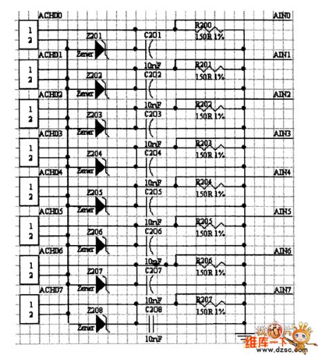
The main features that the analog front-end system is the sensor, which sent the standard signal (ie, 4mA ~ 20mA). This design has certain versatility. As long as the front-end connection is with different sensors, different signal sources can be collected. As the reference for the A / D converter is voltage, which refers that the reference source is the voltage, the A / D achieves voltage conversion. Such requires the conversion from a current signal to a voltage signal. The picture shows the concrete analog acquisition circuit.
It can be seen from the figure that the acquisition circuit convert a current signal into a voltage signal through a resistor. In order to improve the progress of collection, high-precision resistors are needed. Resistors with 1% precision is used here.
(View)
View full Circuit Diagram | Comments | Reading(616)
Reset circuit with a piece of MAX809 chip
Published:2011/6/19 1:42:00 Author:John | Keyword: chip
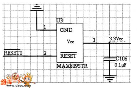
In the SCM system, SCM needs reset circuit. The reset circuit can be reset circuit using R-C circuit and also can be reset circuit using reset chip. R-C reset circuit is economic but is not reliable. The reset circuit using reset chip is with high reliability. So in order to ensure the reliability of the reset circuit system, the ystem uses a MAX809 chip. Reset circuit is as shown in the figure.
In order to reduce the interference of the power supply, a 0.1μF capacitor is needed to be added on the input legs of the reset chip's power supply, thus achieving the filtering function and reducing the interference for the input end.
(View)
View full Circuit Diagram | Comments | Reading(1245)
Microcontroller circuit
Published:2011/6/19 1:33:00 Author:John | Keyword: Microcontroller
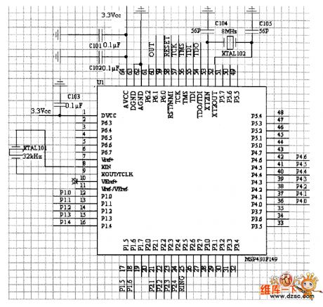
Microcontroller circuit is as the core control part of the whole system. It notably completies the interface with other circuits, resulting in processing the data. The processing results can be come out in some way, such as being displayed or alarmed. The picture shows the microcontroller circuit.
It can be seen through the figure that microcontroller’s interface circuit is very simple. The general I / 0 interface of microcontroller is respectively connected with interfacs of other circuits. The design of the clock in the microcontroller chip has some other differences with other microcontrollers. MSP430F149 microcontroller has two clock inputs, whose one is a 32kHz clock signal and the other one is an 8MHz clock signal. (View)
View full Circuit Diagram | Comments | Reading(739)
Systematic temperature acquisition circuit
Published:2011/6/19 0:54:00 Author:John | Keyword: temperature acquisition
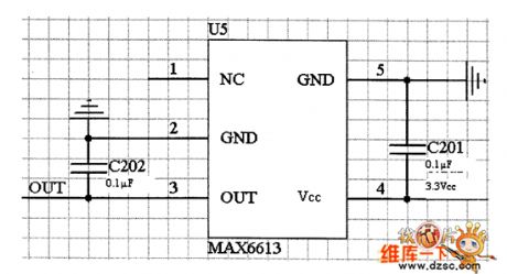
It can be seen through the figure that acquisition circuit is simple and practical.To reduce the effects from the power supply’s input ripple, a 0.1μF capacitor is added on the pin of the power supply so as to achieve filtering function. Thus the disruption for the input end can be reduced.
figure: Systematic temperature acquisition circuit (View)
View full Circuit Diagram | Comments | Reading(502)
system display circuit
Published:2011/6/17 11:28:00 Author:John | Keyword: system display
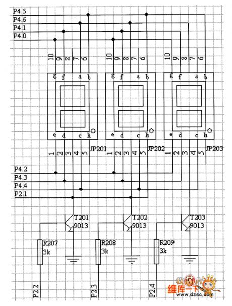
It can be seen from the figure, the display circuit is directly connected with the MCU data I / O port. As MSP430F149 has a wealth of I / O port resources, such parallel interface mode is very easy. Such reduces complexity of system’s design and also increases the reliability of the system. P4.0 ~ P4.6 is used to display data, P2.1 is used to control the display of the decimal point and P2.2, P2.3 and P2.4 are used to control strobe state of the digital tube. If it is expected to be displayed on DIS0, high electricity level is given on pin of P2.2 and strobe state can be displayed through transistor digital tube.
figure: system display circuit (View)
View full Circuit Diagram | Comments | Reading(609)
The clamping amplifier circuit
Published:2011/6/23 21:32:00 Author:Seven | Keyword: clamping amplifier circuit
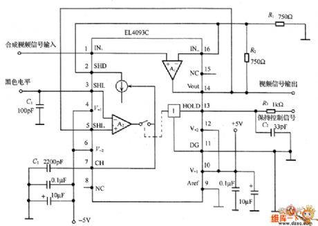
In the figure is the clamping amplifier circuit, which is convenient to connect with other circuits. In the distribution of broadcast or all kinds of analog video signals, it is the simplest communication coupling method, for this method, the clamping amplifier is firstly needed to reappear the DC signals. To traditional clamping amplifier, its input terminal is in capacitor coupling way, when using this coupling method, the DC LEV is regulated by forcing the capacitor to discharge during the level blanking period.
(View)
View full Circuit Diagram | Comments | Reading(808)
HA1394--The 6-8W dual audio power amplifier circuit
Published:2011/6/23 21:12:00 Author:Seven | Keyword: audio power amplifier
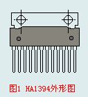
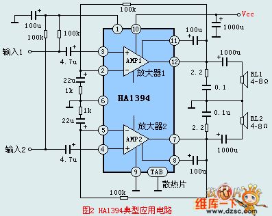
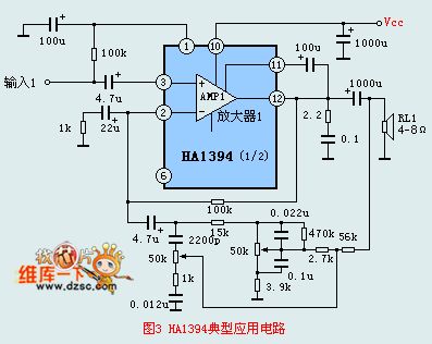
HA1394 is the 6-8W dual audio power amplifier circuit, which is produced by Hitachi, Japan. when Vcc=25V and RL=8Ω, the output power of each channel is 8.2w, THD=15%. The circuit is suitable for compounded stereo system and TV audio amplifier, HA1394 is in 12-lead single in-line plastic package, the outline is shown in figure 1.Circuit features:1. Dual audio power amplifier:7-8.2W/channel; 2.few external components(11 capacitors and 6 resistors);3.wide working voltage range, 18-35v; 4. Low noise, low distortion; 5. There is the protection circuit in it.
(View)
View full Circuit Diagram | Comments | Reading(2852)
The timing circuit composed of TC9160
Published:2011/6/23 1:31:00 Author:qqtang | Keyword: timing circuit
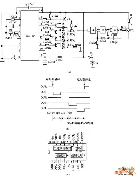
In the figure is the timing circuit composed of TC9160. Generally, a timing circuit discharges with capacitors, as the charge/discharge is not in linearity, so the time is not the evenly spaced scale. Besides, if we want to acquire a timing over 10 min, we need capacitors of more than 1000μF and resistors of several hundred MΩ. Though the NE555 timer circuit is simple, but it needs capacitors of little leakage and large insulated resistance.
TC9160 is an integrated circuit contains frequency splitting counters, its working voltage is low, which is 1.8v. Its consuming current is low. (View)
View full Circuit Diagram | Comments | Reading(1023)
The timing circuit composed of HDl4538
Published:2011/6/21 22:00:00 Author:qqtang | Keyword: timing circuit
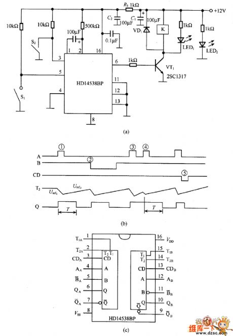
In the figure is the timing circuit composed of HDl4538. HDl4538 has many features, for example, when its single steady multi-resonance oscillator is used as the timer, both the positive edge or the passive edge of the pulse can trigger the circuit; the consuming current is low, when the working voltage is 15v, the current is only 15nA; the range of the working voltage is wide, which is 3~18v; the timing set is irrelevant to the working voltage, which is only decided by the external capacitors and the resistance values, the resistance can be 5kΩ~∞, the capacitance is 2000pF~∞.
HDl4538 contains 2 single steady multi-resonance oscillators. (View)
View full Circuit Diagram | Comments | Reading(616)
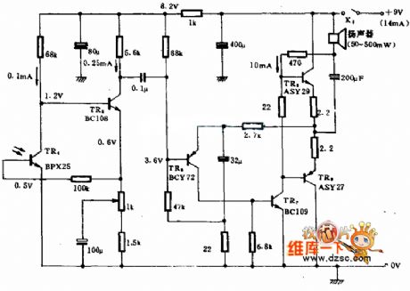
The photo-communication receiver circuit
Published:2011/6/17 0:15:00 Author:Seven | Keyword: photo-communication receiver
View full Circuit Diagram | Comments | Reading(646)
The STK4191 application circuit
Published:2011/6/20 21:56:00 Author:Seven | Keyword: application circuit
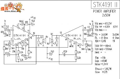
The STK4191 application circuit is shown in the figure.
(View)
View full Circuit Diagram | Comments | Reading(7641)
The STK4182 application circuit
Published:2011/6/20 21:59:00 Author:Seven | Keyword: application circuit
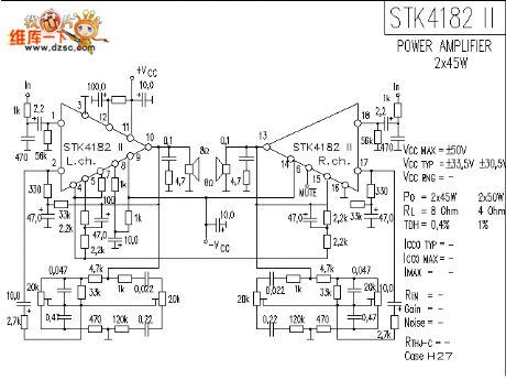
The STK4182 application circuit is shown in the above figure.
(View)
View full Circuit Diagram | Comments | Reading(7963)
The EL8+AD1/400 low power single terminal circuit
Published:2011/6/20 21:59:00 Author:Seven | Keyword: low power, single terminal
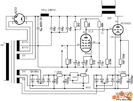
The EL8+AD1/400 low power single terminal circuit is shown in the above figure.
(View)
View full Circuit Diagram | Comments | Reading(1324)
| Pages:193/250 At 20181182183184185186187188189190191192193194195196197198199200Under 20 |
Circuit Categories
power supply circuit
Amplifier Circuit
Basic Circuit
LED and Light Circuit
Sensor Circuit
Signal Processing
Electrical Equipment Circuit
Control Circuit
Remote Control Circuit
A/D-D/A Converter Circuit
Audio Circuit
Measuring and Test Circuit
Communication Circuit
Computer-Related Circuit
555 Circuit
Automotive Circuit
Repairing Circuit