
Control Circuit
Index 258
SONY KV2184 switch power supply circuit
Published:2011/5/23 22:35:00 Author:John | Keyword: switch
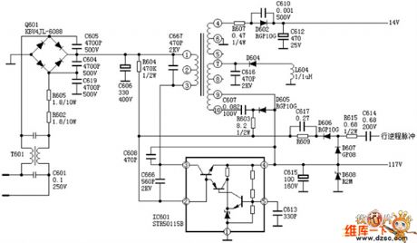
SONY KV2184 switch power supply circuit is shown below.
(View)
View full Circuit Diagram | Comments | Reading(1706)
Emitter follower reference circuit
Published:2011/5/26 2:30:00 Author:Christina | Keyword: Emitter follower, reference circuit
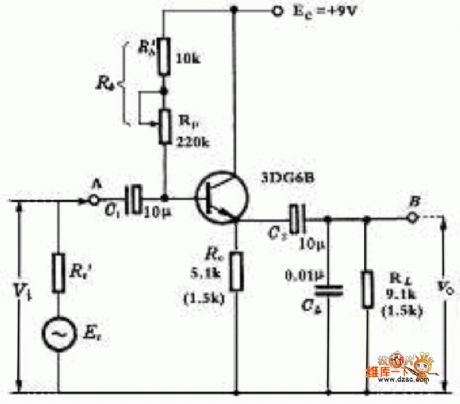
The Emitter follower reference circuit
(View)
View full Circuit Diagram | Comments | Reading(823)
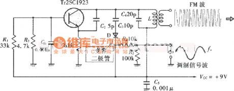
Direct FM Modulation Circuit Composed of Variable Capacitance Diode
Published:2011/5/25 4:47:00 Author:Joyce | Keyword: Direct FM Modulation, Variable Capacitance Diode
View full Circuit Diagram | Comments | Reading(709)
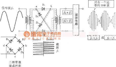
Annular Modulation Circuit
Published:2011/5/25 4:49:00 Author:Joyce | Keyword: Annular , Modulation
View full Circuit Diagram | Comments | Reading(593)
555 light control timing streetlight circuit
Published:2011/5/22 5:06:00 Author:TaoXi | Keyword: light control, timing, streetlight
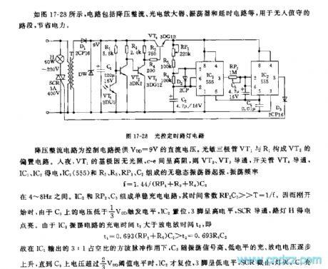
The step-down rectifier circuit supplies the VDD=9V DC voltage to the control circuit, the biasing circuit of VT2 is composed of the phototransistor VT1 and R1. At night, the base electrode has no light, so c-e has the high resistance, VT2, VT3 and the switch tube VT4 conduct, IC1,IC2 get the power, the astable oscillator which is composed of the IC1(555) and R5,R6,RP1,C2 starts to work. The oscillation frequency f=1.44/(RP1+R5+R6)C2. The monostable charging circuit is composed of the IC2 and RP2,C3, the time constant Rp2C3>>T=1/f. At the beginning, the voltage of C3 is lower than 1/3VDD trigger electrical level, so IC2 sets, pin-3 has the high electrical level, SCR conducts and the street lamp H turns on.
(View)
View full Circuit Diagram | Comments | Reading(680)
555 light control street lamp switch circuit
Published:2011/5/24 2:53:00 Author:TaoXi | Keyword: light control, street lamp, switch circuit
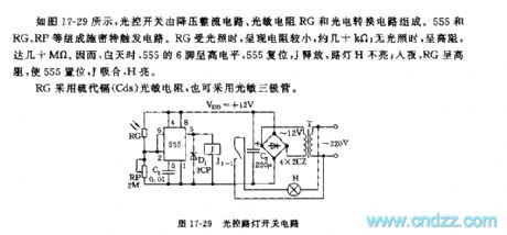
As the figure 17-29 shows, the light control is composed of the step-down rectifier circuit, the photoconductive resistance RG and the photoelectric conversion circuit. The Schmitt trigger circuit is composed of the 555 and the RG,RP.etc. RG receives the light, so it has the low resistance about dozens of thousands of ohms; when there is no light, RG has the high resistance about dozens of megabytes of ohms. So in the daytime, pin-6 of 555 has the high electrical level, 555 resets, J releases, the street lamp H turns off; at night, RG has the high electrical level, 555 sets, J closes, the street lamp H turns on.RG uses the Cds photoconductive resistance, also it can use the phototransistor.
(View)
View full Circuit Diagram | Comments | Reading(657)
555 light control streetlights circuit
Published:2011/5/22 9:10:00 Author:TaoXi | Keyword: light control, streetlights
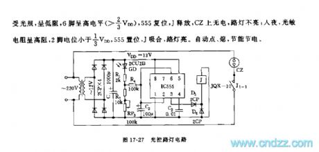
As the figure 17-27 shows, the light control circuit uses the photosensitive components and the 555.etc to form the trigger circuit. In the daytime, the 2CU2B photoconductive resistance receives the illumination, so it has the low resistance, pin-6 has the high electrical level (>2/3VDD), 555 resets, J releases, CZ has no power, so the streetlight turns off; at night, the photoconductive resistance has the high resistance, pin-2's electrical level is less than 1/3VDD, 555 sets, J closes, the streetlight turns on.
(View)
View full Circuit Diagram | Comments | Reading(630)
555 photo amplification automatic metering timer circuit
Published:2011/5/23 4:03:00 Author:TaoXi | Keyword: photo amplification, automatic metering, timer
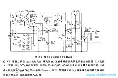
As the figure 17-9 shows, the timer is composed of the photosensitive sensor head, the 555 and the C2, C4~C7.etc. And this circuit can be used in wide range of applications such as the photo amplification automatic metering timer.
The photosensitive sensor uses the phototransistor 3DU type, when K1 is in the position of AE 1 , you press AN, the 555 sets, VT4 conducts, J closes, and the amplifier light turns on, the exposure starts. The photodiode injects different kinds of current to VT3 according to the strength of the enlarging paper's reflected light. So the time of pin-6 charges to the 2/3VDD threshold level is different.
(View)
View full Circuit Diagram | Comments | Reading(578)
555 photographic exposure timer circuit
Published:2011/5/23 5:30:00 Author:TaoXi | Keyword: photographic, exposure, timer circuit
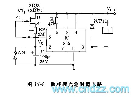
As the figure 17-8 shows, the timer uses the 555 as the core. If you press switch AN, the timing begins. You need to press AN to set the 555's trigger port,pin-3 has the high electrical level, the normally closed contact point of the relay will turn on the expose lamp. Then the C is charged through VT1 and RP. In order to make the charging voltage to keep the linear growth, we use the MOSFET 3DJ8 for the cross-flow charging. When C's charging voltage is higher than pin-6's threshold level 2/3VDD, 555 resets, pin-3 has the low electrical level.
(View)
View full Circuit Diagram | Comments | Reading(884)
555 household automatic lighting switch
Published:2011/5/22 18:57:00 Author:TaoXi | Keyword: household, automatic, lighting switch
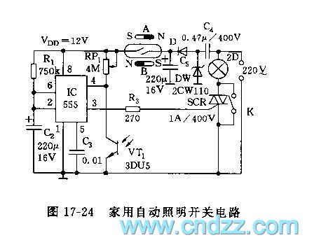
As the figure 17-24 shows, you can use the photosensitive sensor and the magnetic switch to control 555's trigger state and power supply, at night, this circuit can automatically open and auto-off delay.
The city electricity is stepped down and rectified by the circuit, then it becomes the 12V voltage to supply the 555. The controllable trigger delay circuit is composed of the 555 and R1,C2,VT1, RP1. In the day time, the VT1(3DU5) is in the low resistance state because of the illumination, so the 555's pin-4 has the low electrical level (<0.7V), the 555 is forced to reset, pin-3 has the low electrical level, SCR cuts off.
(View)
View full Circuit Diagram | Comments | Reading(923)
555 hepatitis germs disinfector control circuit
Published:2011/5/23 20:15:00 Author:TaoXi | Keyword: hepatitis, germs, disinfector, control circuit
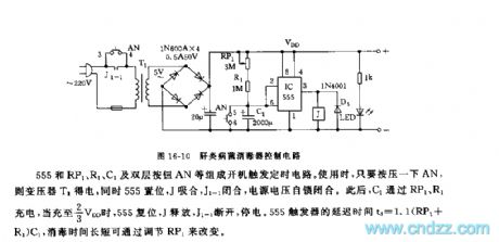
As the figure 16-10 shows, this disinfector control circuit is composed of the step-down rectifier circuit (VDD=+6V), the 555 boot timing circuit and the control circuit. It can be used to control the timing time of the sodium hypochlorite production.
The boot trigger timing circuit is composed of the 555, RP1,R1,C1 and the double-deck button AN. When you are using it, press AN, the transformer T1 gets the power, and 555 sets, J and J1-1 close, the power supply voltage self-locking closes. And then, C1 is charged through RP1 and R1, when C1 is charged to 2/3VDD, 555 resets, J releases, J1-1 cuts off, there is no power supply. The 555 trigger's delay time td=1.1(RP1+R1)C1, you can change the length of the sterilization time by adjusting RP1.
(View)
View full Circuit Diagram | Comments | Reading(564)
Motor electronic speed controller circuit diagram 1
Published:2011/5/19 1:35:00 Author:Lucas | Keyword: Motor, electronic speed controller
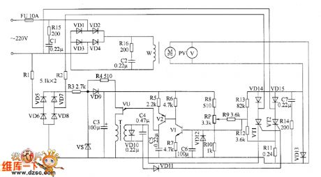
The motor electronic speed controller circuit consists of power supply circuit, excitation circuit, trigger circuit and speed control circuit, the circuit is shown as the chart. Power supply circuit consists of the fuse FU, resistors R1 ~ R3, rectifier diodes VD5 ~ VD9, Zener diode VS and filter capacitor C3. Excitation circuit consists of resistors R15 and R16, capacitors C1, C2 and diodes D1 ~ D4. Trigger control circuit is composed of the pulse transformer T, single-junction transistor VU, transistors V1, V2, diodes VD10 ~ VD12, capacitors C4 ~ C6 and resistors R4 ~ R7. Speed control circuit consists of the intergranular tubes VT1, VT2, diodes VD13 ~ VD15, resistors R8 ~ R14, capacitor C7 and potentiometer RP.
(View)
View full Circuit Diagram | Comments | Reading(2207)
Motor protector circuit diagram 18
Published:2011/5/20 20:35:00 Author:Lucas | Keyword: Motor protector
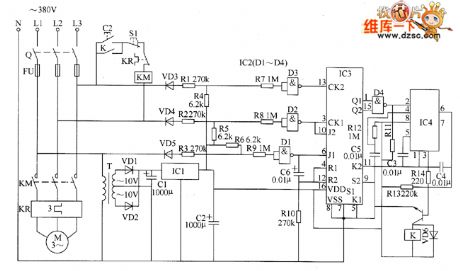
The motor protection circuit is composed of the power circuit, phase sequence detection circuit, monostable circuit and control implementation circuit, the circuit is shown as the chart. Power circuit is composed of the power transformer T, rectifier diodes VD1, VD2, capacitors C1, C2, and three-terminal voltage regulator integrated circuit IC1. Phase sequence detection circuit is composed of the diodes VD3 ~ VD5, resistors R1 ~ RIO, capacitor C6, four NAND gate Schmitt trigger integrated circuit IC2 (D1 ~ D4) and dual JK master-slave flip-flop integrated circuit IC3. Monostable circuit is composed of the resistors R11 ~ R13, capacitors C3 ~ C5 and time-based integrated circuit IC4. Control implementation circuit is composed of the resistor R14, transistor V, diode VD6 and relay K and other components. Knife switch Q, fuse FU, AC contactor KM and KR form the origin control circuit of motor M .
(View)
View full Circuit Diagram | Comments | Reading(3242)
Motor protector circuit diagram 16
Published:2011/5/20 21:04:00 Author:Lucas | Keyword: Motor protector
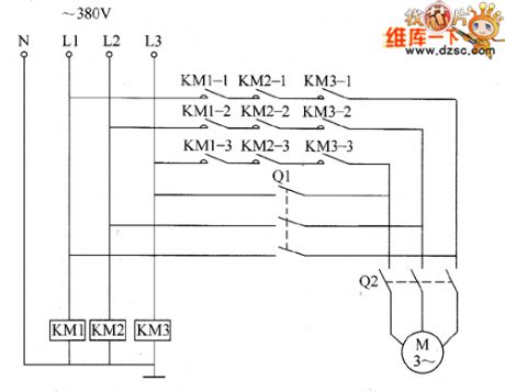
The motor protector circuit is composed of the AC contactors KM1 ~ KM3, knife switches Q1, Q2 and motor M, the circuit is shown as the chart. When 380V AC supply voltage is normal, the AC contactors KM1 ~ KM3 get power and pull in, their 3 groups of normally open contacts are connected, then closing the knife switch Q2 will make motor M get power and operate. When the AC 380V voltage is open-phase because of thunder or other reasons, one contactor of KM1 ~ KM3 couldn't pull in or get power, the power supply circuit of motor M will cut off to protect the motor M. For example, the voltage on L2 phase line disappears, AC contactor KM2 releases, the normally open contacts KM2-1 ~ KM2-3 cut off. KM1 ~ KM3 select the 220V AC voltage contactor.
(View)
View full Circuit Diagram | Comments | Reading(905)
Motor protector circuit diagram 15
Published:2011/5/20 22:03:00 Author:Lucas | Keyword: Motor protector
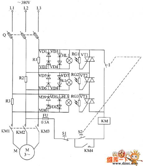
The motor protector circuit detection circuit is composed of the current sampling circuit and light control protection circuit, the circuit is shown as the chart. Current sampling detection circuit consists of sampling resistors R1 ~ R3. Light control protection circuit is composed of the protection diodes VD1 ~ VD12, small bulbs HL1 ~ HL3, photosensitive resistors RC1 ~ RC3 and thyristors VT1 ~ VT3. Q is the fuse knife switch, FU is fuse, S1 is stop button, S2 is the start button, KM is the AC contactor. R1 ~ R3 select 5 ~ 1OW wire wound resistors, the resistance should be based on the rated power of motor. If it uses 1.5kW motor, the rated current is about 3A, the sampling resistors can be set at 0.3Ω. RG1 ~ RG3 use MC45 series of light-sensitive resistors. VD1 ~ VD12 use 1N5408 silicon rectifier diodes. VT1 ~ VT3 select MAC97A6 bidirectional thyristors.
(View)
View full Circuit Diagram | Comments | Reading(795)
Motor electronic speed controller circuit diagram 3
Published:2011/5/20 20:06:00 Author:Lucas | Keyword: Motor , electronic speed controller
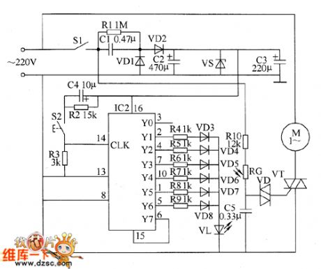
The motor electronic speed controller circuit consists of power supply circuit, counter and the light control pulse width modulation circuit, the circuit is shown as the chart. Power supply circuit is composed of the switch S1, step-down capacitor C1, resistor R1, rectifier diodes VD1 and VD2, Zener diode VS and filter capacitors C2, C3. IC2 is the decimal counter IC, its pin 14 (CLK-side) is the count pulse signal input and connceted the resistors R3 and button S2. When people press S2 each time, pin 14 of IC2 will input a count pulse, when people press S2 continuously, the Y1 ~ Y6 output end of IC2 will output high level in the turn. The resistors R4 ~ R9 are gradually increasing, when the different output ends output high level, the current flowing the LED is different to make the brightness of VL1 being gradually weaking from strong.
(View)
View full Circuit Diagram | Comments | Reading(1416)
Motor protector circuit diagram 8
Published:2011/5/21 1:44:00 Author:Lucas | Keyword: Motor protector
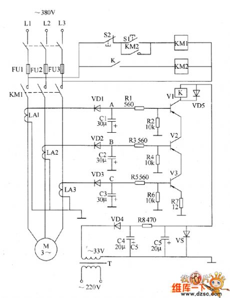
The motor protection circuit is composed of power supply circuit, current detection circuit and protection control circuit, the circuit is shown as the chart. Power circuit is composed of the power transformer T, rectifier diode VD4, filter capacitors C4, C5, current limiting resistor R8 and Zener diode VS and other components, the circuit is used to generate +20 V voltage for relay K and its drive circuit. Current detection circuit is composed of the current transformers LA1, LA2, LA3, and rectifier diodes VD1 ~ VD3, filter capacitors C1 ~ C3 and other components. The protection control circuit is composed of resistors R1 ~ R7, transistors V1 ~ V3, relay Κ, AC contactors KMI and KM2 and start button S1, stop button S2. After people press the start button S1, AC power contactor KM1 works, the three contacts are connected, the motor M operates.
(View)
View full Circuit Diagram | Comments | Reading(1971)
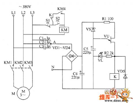
Motor protector circuit diagram 7
Published:2011/5/21 1:26:00 Author:Lucas | Keyword: Motor protector
When the three-phase power supply is normal, the public contact 0 of detection capacitor C1 ≈ C3 has no current flowing, the two ends of C4 have no voltage, and the crystal tube VT is off, the relay K does not pull in, its normally closed contact is connected, the LED VL does not emit light, the motor M operates normally (in fact, the three-phase voltage unbalance, or the capacity of C1 ~ C3 differ will cause O point having a small current to flow, but the K doesn't move.) KR is the thermal relay, S1 is the Close button, S2 is the start button, R is the current limiting resistor. Potentiometer RP, capacitor C5 or intergranular tube VT form delay circuit to prevent serious harmonic interference or instantaneous voltage fluctuations and protector's malfunction. RP's positive adjustment value can change the conduction delay time of VT (generally 0.5 ~ 1s).
(View)
View full Circuit Diagram | Comments | Reading(685)
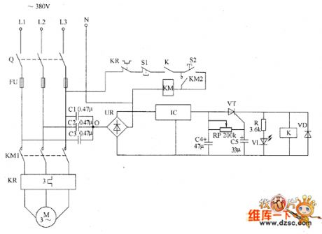
Motor protector circuit diagram 10
Published:2011/5/21 10:38:00 Author:Lucas | Keyword: Motor protector
The motor protector circuit is composed of voltage detection circuit and protection control implementation circuit, the circuit is shown as the chart. Starting control circuit is composed of stop button S1, start button S2, AC contactor KM ( the original motor starting circuit). Voltage detection circuit is composed of the diodes VD1 ~ VD3, voltage regulator diodes VS1 ~ VS3, resistors R1 ~ R6, capacitors C1 ~ C3 and optocouplers VLC1 ~ VLC3. Protection control circuit consists of transistors V, relay K, diode VD4 and resistor R7. If one phase of the three-phase AC power is open-phase, the optocoupler in voltage detection circuit is turning off, V could not turn on, K does not pull in, disconnecting S2 will make KM released immediately to achieve fault phase automatic protection purpose. R1, R3 and R5 use 1 ~ 2W metal film resistors.
(View)
View full Circuit Diagram | Comments | Reading(1370)
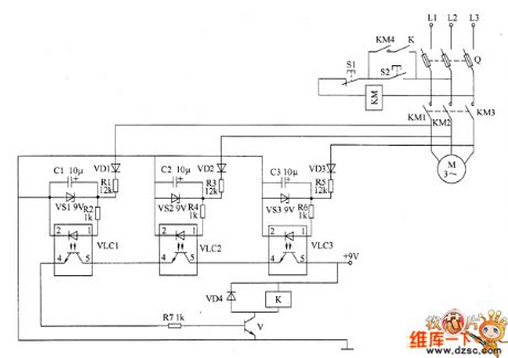
Motor protector circuit diagram 11
Published:2011/5/21 10:28:00 Author:Lucas | Keyword: motor protector
The motor protector circuit consists of capacitors C1 ~ C5, diodes VD1 ~ VD5, resistors R1, R2, zener diode VS, light-emitting diode VL, single-junction transistor VU and relay K, the circuit is shown as the chart. When the three-phase supply of L1 ~ L3 is in the normal, the junction point A on capacitors C1 ~ C3 has the lower AC voltage, the voltage is rectified by the VD1 ~ VD4, filtered by C4, so it is insufficient to turn on VS and VU, k does not pull in, the motor M operates normally. When the three-phase power is restored to normal, after a short delay VU deadline, K releases, then people can press the start button to restart the motor S2. R1 and R2 use 1/4W carbon film resistors or metal film resistors. C1 ~ C3 select CBB capacitors with the voltage being more than 400V: C4 and C5 select electrolytic capacitors, the withstand voltage of C4 is 25V, the withstand voltage of C5 is 16V. VD1 ~ VD5 use 1N4007 silicon rectifier diodes.
(View)
View full Circuit Diagram | Comments | Reading(745)
| Pages:258/312 At 20241242243244245246247248249250251252253254255256257258259260Under 20 |
Circuit Categories
power supply circuit
Amplifier Circuit
Basic Circuit
LED and Light Circuit
Sensor Circuit
Signal Processing
Electrical Equipment Circuit
Control Circuit
Remote Control Circuit
A/D-D/A Converter Circuit
Audio Circuit
Measuring and Test Circuit
Communication Circuit
Computer-Related Circuit
555 Circuit
Automotive Circuit
Repairing Circuit